

Transparent conductive oxide thin film substrate, method of fabricating the same, and organic light-emitting device and photovoltaic cell having the same
- Summary
- Abstract
- Description
- Claims
- Application Information
AI Technical Summary
Benefits of technology
Problems solved by technology
Method used
Image

Examples
Embodiment Construction
[0040]Reference will now be made in detail to a transparent conductive oxide thin film substrate, a method of fabricating the same, and an organic light-emitting device (OLED) and photovoltaic cell having the same according to the present invention, embodiments of which are illustrated in the accompanying drawings and described below, so that a person having ordinary skill in the art to which the present invention relates can easily put the present invention into practice.
[0041]Throughout this document, reference should be made to the drawings, in which the same reference numerals and signs are used throughout the different drawings to designate the same or similar components. In the following description of the present invention, detailed descriptions of known functions and components incorporated herein will be omitted when they may make the subject matter of the present invention unclear.
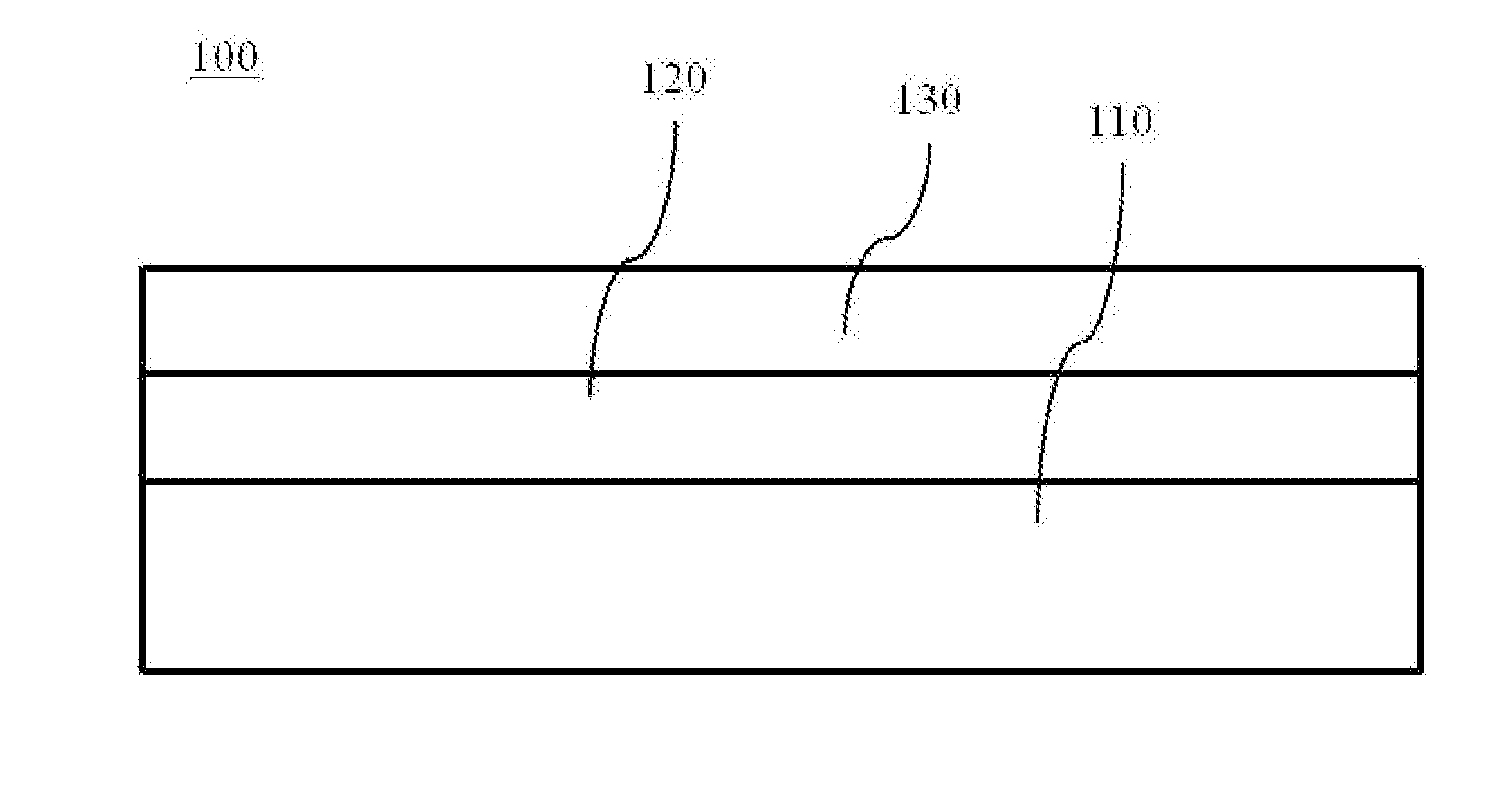
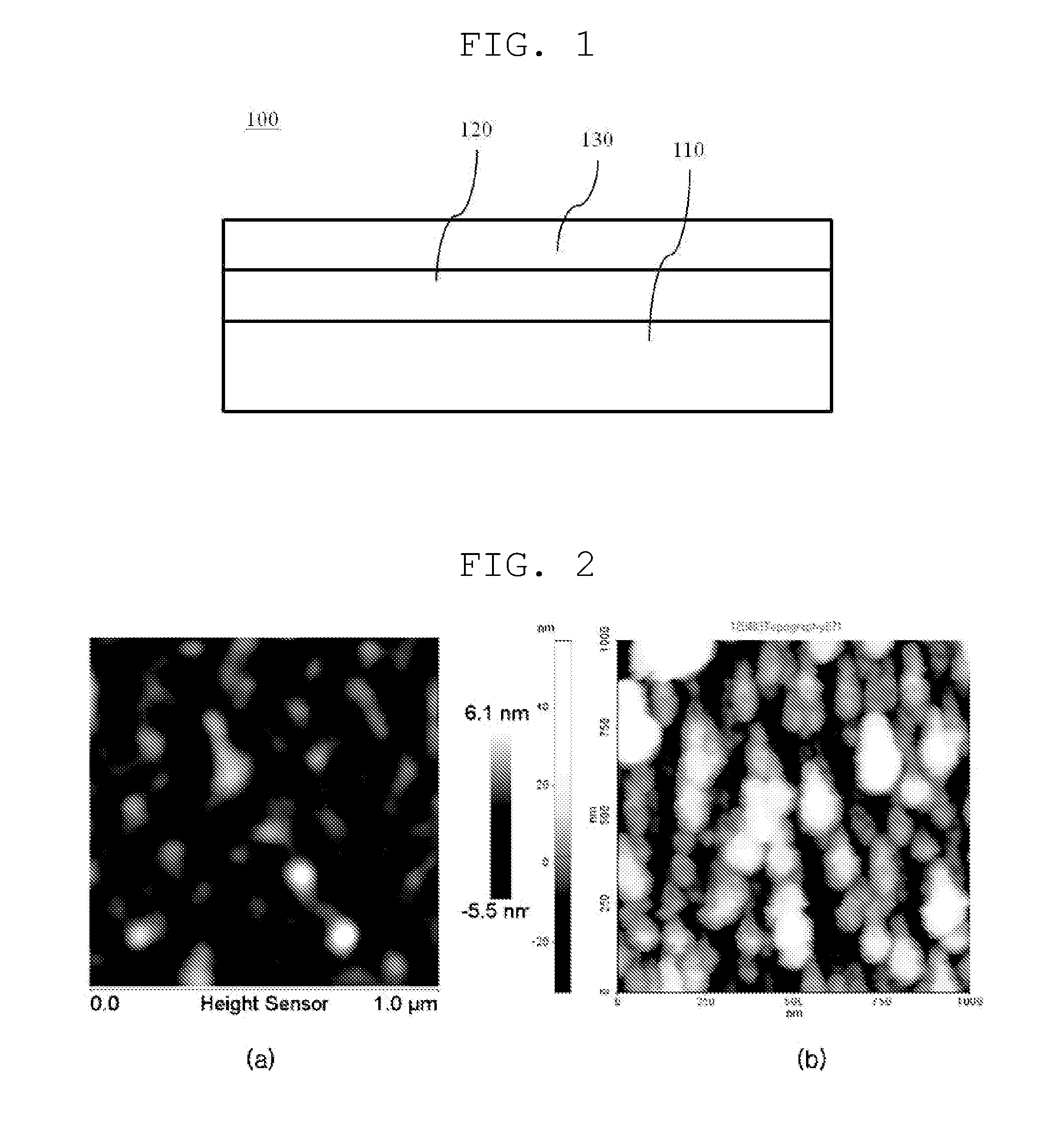
[0042]As shown in FIG. 1, a transparent conductive oxide thin film substrate 100 according to...
PUM
| Property | Measurement | Unit |
|---|---|---|
| Fraction | aaaaa | aaaaa |
| Fraction | aaaaa | aaaaa |
| Thickness | aaaaa | aaaaa |
Abstract
Description
Claims
Application Information