Soi substrate and method for manufacturing soi substrate

a technology of soi substrate and substrate layer, which is applied in the direction of basic electric elements, electrical apparatus, semiconductor devices, etc., can solve the problems of local peeling at the bonding surface, unfavorable phenomenon, etc., and achieve the effect of suppressing the thermal distortion induced during a corresponding heat treatment process, suppressing surface roughness, and excellent in surface flatness and in-plane film thickness uniformity

Active Publication Date: 2010-02-04
SHIN ETSU CHEM IND CO LTD
View PDF7 Cites 11 Cited by
  • Summary
  • Abstract
  • Description
  • Claims
  • Application Information

AI Technical Summary

Benefits of technology

[0025]In the present invention, the temperature for bonding of a transparent insulating substrate and a single crystal Si substrate after formation of a hydrogen ion implantation layer is set to 350° C. or below. Accordingly, the amount of thermal distortion induced during a corresponding heat treatment process is suppressed, and an undesirable phenomenon due to the differences in physical property values between the single crystal Si substrate and the transparent insulating substrate, such as a substrate fracture or local peeling at bonding surfaces, can be avoided.
[0026]Since a heat treatment temperature of 350° C. or below is sufficiently low compared to a temperature required to change the state of bonds of a silicon atom, local damage in the hydrogen ion implantation layer induced by ion implantation is maintained during a corresponding heat treatment process. It is thus possible to obtain an SOI layer with suppressed surface roughness after peeling.
[0027]An SOI substrate thus obtained is excellent in surface flatness and in-plane film thickness uniformity and has few structural defects which cause light scattering. Therefore, it is possible to provide an SOI substrate especially suitable for manufacturing an optical device.

Problems solved by technology

However, if an SOI substrate is manufactured by bonding together a single crystal silicon substrate and a transparent insulating substrate (e.g., a quartz substrate), since the differences in thermal expansion coefficient and mechanical strength (a modulus of rigidity or the like) between the two substrates to be bonded together are large, heat treatment at a high temperature as described above causes trouble.
More specifically, an undesirable phenomenon such as a fracture in a one with lower rigidity of the substrates (often the transparent insulating substrate) or local peeling at bonding surfaces may occur.

Method used


Image

  • Soi substrate and method for manufacturing soi substrate
  • Soi substrate and method for manufacturing soi substrate
  • Soi substrate and method for manufacturing soi substrate

Examples


example 1

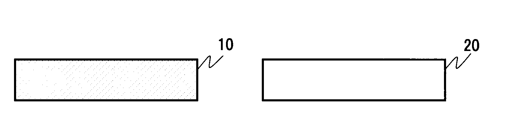
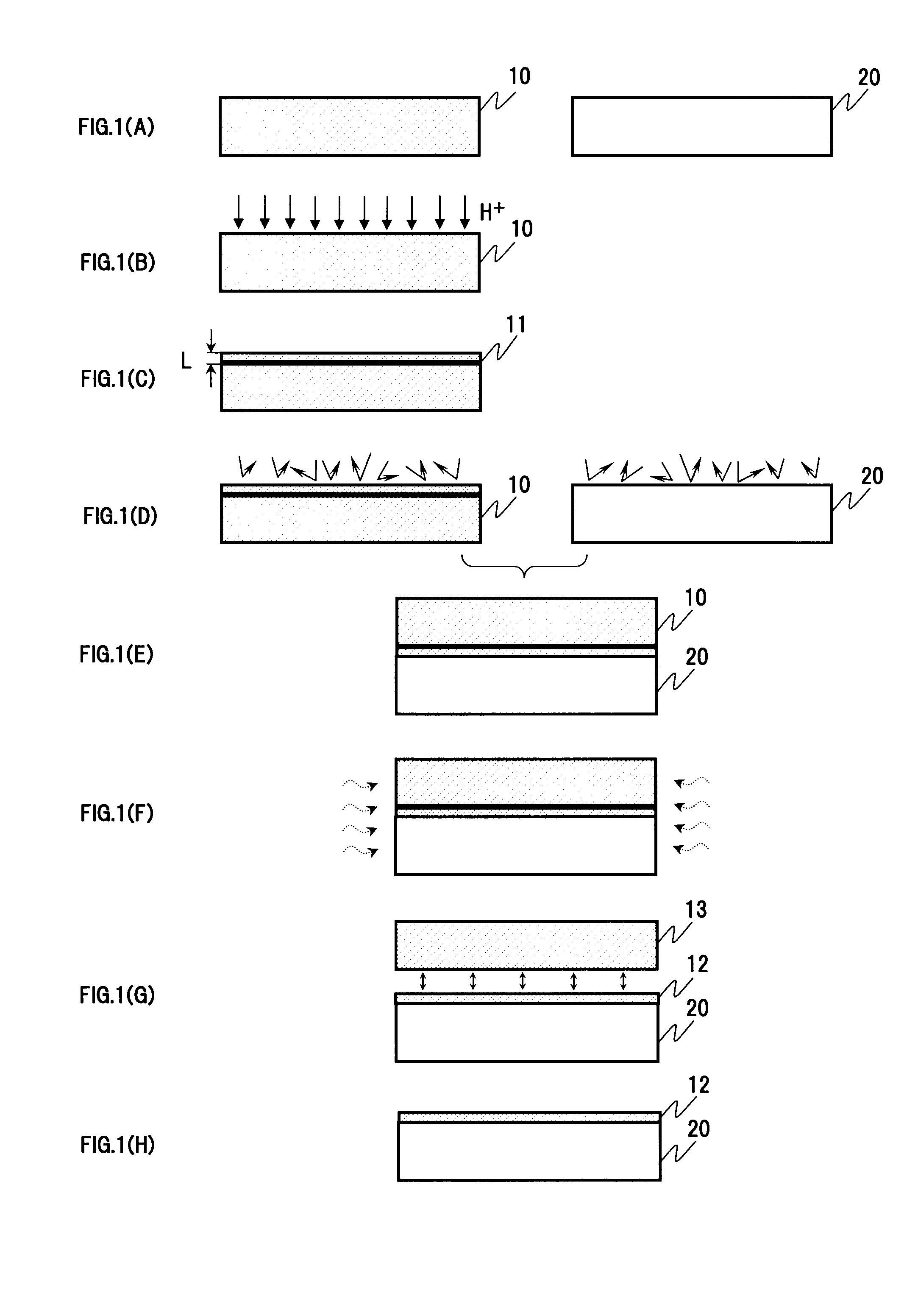
[0038]FIGS. 1(A)-1(H) show views for explaining an example of a manufacturing process for an SOI substrate according to the present invention. First, a single crystal Si substrate 10 and a transparent insulating substrate 20 having the same diameter are prepared (FIG. 1(A)). The single crystal Si substrate 10 is a commercially available Si substrate which is formed through growth by, e.g., the CZ method (Czochralski method). The electrical characteristics such as conductivity type and resistivity, crystal orientation, and crystal diameter of the single crystal Si substrate 10 are appropriately selected depending on design values and processes for a device for which an SOI substrate according to the present invention is used or the display area of a device to be manufactured and the like.

[0039]As the single crystal Si substrate, a substrate of “nearly perfect crystal (NPC)”, single crystal silicon grown by the CZ method (Czochralski method) or the floating zone method (FZ method) may...

example 2

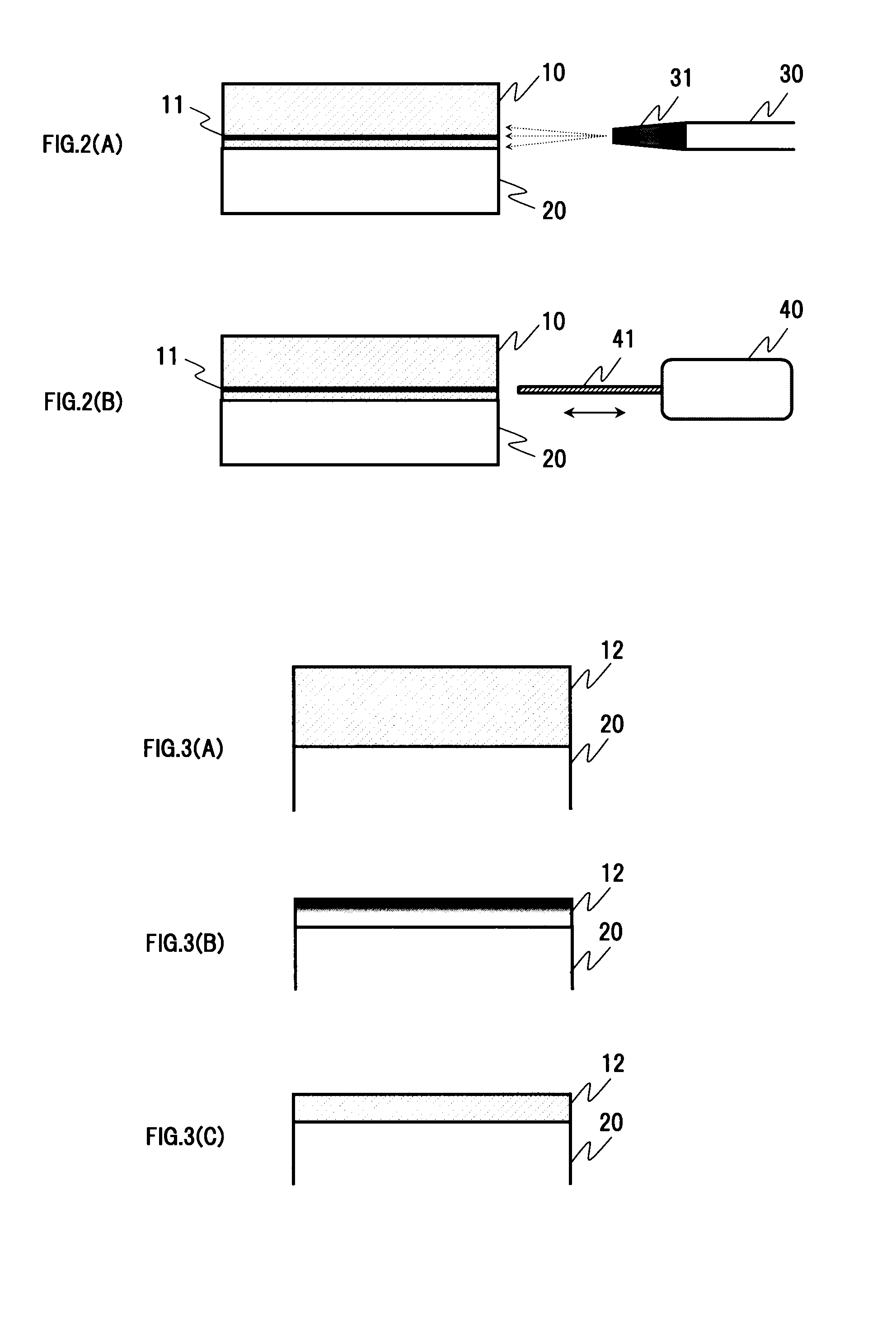
[0064]Although an insulating layer such as a thermal oxide film is not provided on the bonding surface of the single crystal Si substrate used in Example 1, an SOI layer may be formed using a single crystal Si substrate having an oxide film formed in advance on a surface.

[0065]A single crystal Si substrate used in this example is one having a thermal oxide film with a thickness of 100 nm formed on the side of a bonding surface and having a diameter of 200 nm (8 inches). Note that the surface roughness of the thermal oxide film was expressed as an Ra value for a 10 μm×10 μm measurement area obtained by an atomic force microscope and was 0.2 nm.

[0066]As a transparent insulating substrate to be bonded to the single crystal Si substrate, a quartz substrate with a diameter of 200 mm (8 inches) is used. A bonding surface of the transparent insulating substrate is subjected to polishing, and the surface roughness thereof is 0.19 nm in Ra value. Note that a surface roughness measurement con...


PUM

PropertyMeasurementUnit
temperatureaaaaaaaaaa
roughnessaaaaaaaaaa

Abstract

On the side of a surface (the bonding surface side) of a single crystal Si substrate, a uniform ion implantation layer is formed at a prescribed depth (L) in the vicinity of the surface. The surface of the single crystal Si substrate and a surface of a transparent insulating substrate as bonding surfaces are brought into close contact with each other, and bonding is performed by heating the substrates in this state at a temperature of 350° C. or below. After this bonding process, an Si—Si bond in the ion implantation layer is broken by applying impact from the outside, and a single crystal silicon thin film is mechanically peeled along a crystal surface at a position equivalent to the prescribed depth (L) in the vicinity of the surface of the single crystal Si substrate.

Description

TECHNICAL FIELD [0001]The present invention relates to an SOI substrate and a method for manufacturing an SOI substrate and, more particularly, to an SOI substrate in which a peeled surface of a single crystal silicon thin film bonded and formed on a transparent insulating substrate has suppressed surface roughness and a method for manufacturing the SOI substrate.BACKGROUND ART[0002]A so-called SOI (Silicon on Insulator) wafer, in which a single crystal silicon (Si) layer is provided on an insulating film such as an oxide film, is used as a substrate for device formation for the purpose of forming a MOS transistor excellent in radiation-resistant characteristics and latch-up characteristics and excellent at suppressing the short channel effect. Among SOI substrates, a less-defective SOI substrate to which a bonding technique has been applied is attracting attention. The use of such an SOI substrate as a substrate for optical device manufacture has come under review in recent years (...

Claims


Application Information

Patent Timeline
Patent Type & Authority Applications(United States)
IPC IPC(8): H01L21/762H01L27/12
CPCH01L21/76254H01L21/20H01L21/265
Inventor KAWAI, MAKOTOKUBOTA, YOSHIHIROITO, ATSUOTANAKA, KOICHITOBISAKA, YUUJIAKIYAMA, SHOJI
Owner SHIN ETSU CHEM IND CO LTD
Why Eureka
Try Eureka