

Array substrate, manufacturing method thereof, and display device
A technology for array substrates and manufacturing methods, which is applied in semiconductor/solid-state device manufacturing, semiconductor/solid-state device components, instruments, etc., and can solve the problem of large gate off voltage delay, affecting the display effect of display devices, and pulling up gate off voltage, etc. problems, to achieve the effect of eliminating horizontal lines, improving display effects, and avoiding differences
- Summary
- Abstract
- Description
- Claims
- Application Information
AI Technical Summary
Problems solved by technology
Method used
Image


Examples
Embodiment 1
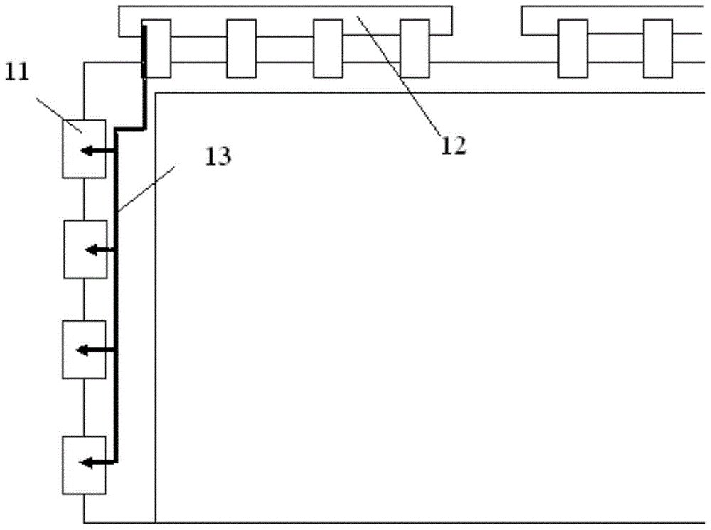
[0061] Such as Figure 7 As shown, multiple Gate COF1s are arranged on the array substrate, and each Gate COF is connected to the DC circuit through the gate driving peripheral wiring VGL1, VGL2, VGL3, and VGL4. In this embodiment, connecting lines can be set on the Gate COF1 B. Connect the adjacent gate drive peripheral wiring through the connection line B on Gate COF1. The material of the connection line B can be metal to meet the low resistance requirement.
[0062] There is no strict requirement on the position of the connection line B, and it is better to keep the length of the connection line B as short as possible, so as to reduce the resistance of the connection line B as much as possible, so that the gate-off voltages of adjacent gate drive peripheral traces tend to be consistent.
Embodiment 2
[0064] Such as Figure 8 As shown, multiple Gate COF1s are arranged on the array substrate, and each Gate COF is connected to the DC circuit through the gate driving peripheral wiring VGL1, VGL2, VGL3 and VGL4. In this embodiment, the wiring area of the array substrate can be A connection line A is provided, and the adjacent gate driving peripheral wiring is connected through the connection line A.
[0065] The connecting line A can be made on the same layer as the gate driving peripheral wiring 2, for example, both are made of a gate metal layer; further, the connecting line A can also be located in a different film layer from the gate driving peripheral wiring, and the connecting line A and the There is an insulating layer between the gate drive peripheral traces, and the connection line A and the gate drive peripheral traces are connected through via holes, so that there is no need to leave a space between the connection line A and the gate drive peripheral traces, and th...
PUM
 Abstract
Description
Claims
Application Information