Enhanced hemt device with back field plate structure and preparation method thereof

A technology of plate structure and back surface field, applied in semiconductor/solid-state device manufacturing, semiconductor devices, electrical components, etc., can solve the problems of discount, difficulty in releasing electrons, etc., and achieve the effect of increasing the breakdown voltage and suppressing the current collapse effect.

Active Publication Date: 2017-02-01
江苏盐综产业投资发展有限公司
View PDF9 Cites 2 Cited by
  • Summary
  • Abstract
  • Description
  • Claims
  • Application Information

AI Technical Summary

Problems solved by technology

However, these problems can only solve the "current collapse" when the device works at low voltage, because at low voltage, electrons only fill the trap states on the semiconductor surface, and when the device works at high voltage, electrons will be more inclined to In order to fill the deep-level trap states in the semiconductor body at the bottom, these deep-level trap states will be more difficult to release electrons than the surface trap states. "Collapse" effect will be greatly reduced

Method used


Image

  • Enhanced hemt device with back field plate structure and preparation method thereof
  • Enhanced hemt device with back field plate structure and preparation method thereof
  • Enhanced hemt device with back field plate structure and preparation method thereof

Examples


Embodiment 1

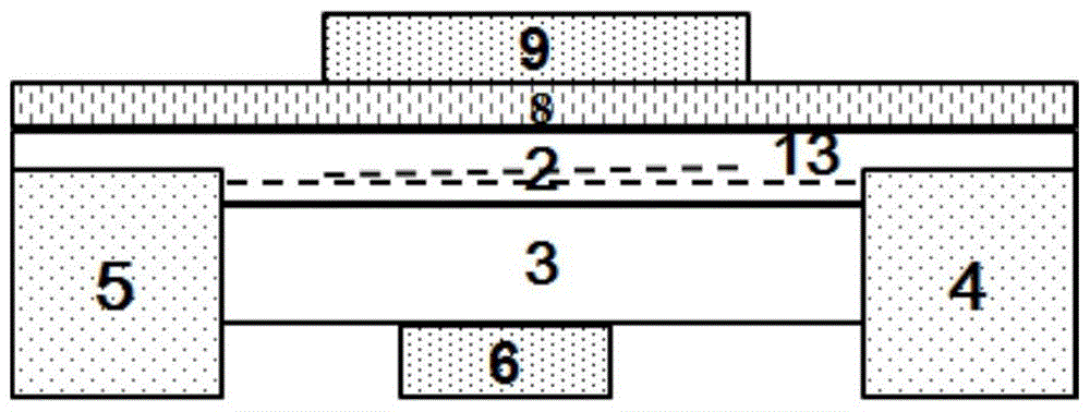
[0056] Example 1 see image 3 , the enhanced HEMT has AlGaN / GaN. GaN is not intentionally doped. AlGaN can be doped with n-type impurities or not. The thickness of AlGaN is about 15 to 30 nm.

[0057] The enhancement mode HEMT has a drain 4 and a source 5 . The drain 4 and the source 5 form an ohmic contact with AlGaN / GaN, and form a good electrical connection with the two-dimensional electron gas in the channel. The drain electrode 4 and the source electrode 5 are ohmic contacts formed by rapid high-temperature annealing of multilayer metals (such as Ti / Al / Ti / Au or Ti / Al / Ni / Au, etc.).

[0058] Further, the enhanced HEMT has a gate 6, between the source 5 and the drain 4, the distance close to the source 5 is relatively short, and the gate 6 is located on AlGaN.

[0059] The back field plate electrode 9 is located on the GaN, overlaps the gate 6 in the vertical direction, and extends to the source 5 and the drain 4 (or only extends to the drain 4 or the source 5, refer t...

Embodiment 2

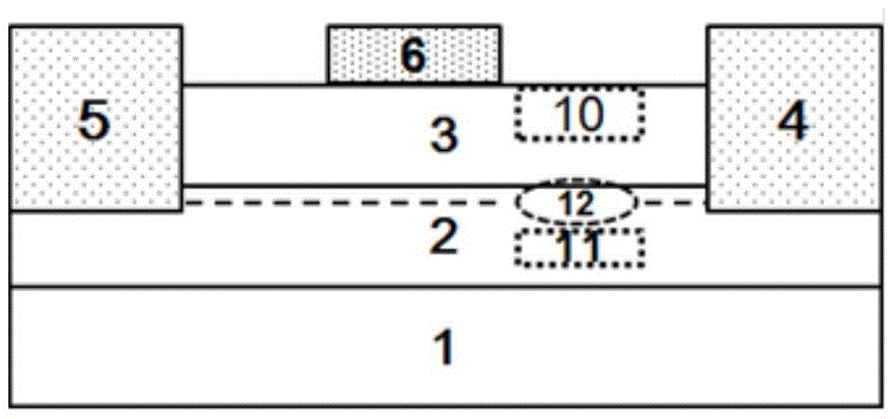
[0065] Example 2 see Image 6 , the enhanced HEMT has AlGaN / GaN. GaN is not intentionally doped. AlGaN can be doped with n-type impurities or not. The thickness of AlGaN is about 15 to 30 nm.

[0066] The enhancement mode HEMT has a drain 4 and a source 5 . The drain 4 and the source 5 form an ohmic contact with AlGaN / GaN, and form a good electrical connection with the two-dimensional electron gas in the channel. The drain electrode 4 and the source electrode 5 are ohmic contacts formed by rapid high-temperature annealing of multilayer metals (such as Ti / Al / Ti / Au or Ti / Al / Ni / Au, etc.).

[0067] Further, the enhanced HEMT has a gate 6, between the source 5 and the drain 4, the distance close to the source 5 is relatively short, and the gate 6 is located on AlGaN.

[0068] The back field plate electrode 9 is located on the GaN, overlaps the gate 6 in the vertical direction, and extends to the source 5 and the drain 4 (or only extends to the drain 4 or the source 5, refer t...

Embodiment 3

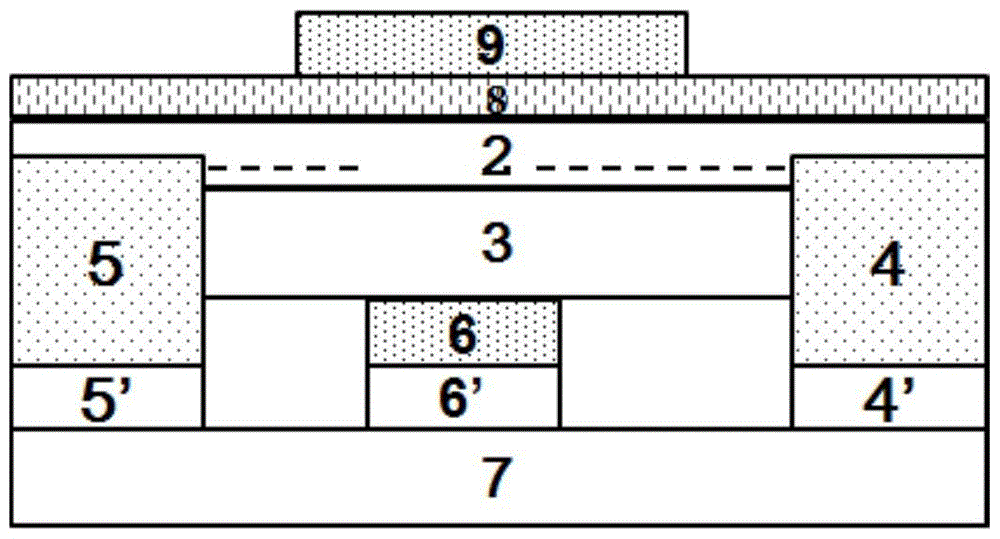
[0074] Example 3 see Figure 7 , the enhanced HEMT has AlGaN / GaN. GaN is not intentionally doped. AlGaN can be doped with n-type impurities or not. The thickness of AlGaN is about 15 to 30 nm.

[0075] The enhancement mode HEMT has a drain 4 and a source 5 . The drain 4 and the source 5 form an ohmic contact with AlGaN / GaN, and form a good electrical connection with the two-dimensional electron gas in the channel. The drain electrode 4 and the source electrode 5 are ohmic contacts formed by rapid high-temperature annealing of multilayer metals (such as Ti / Al / Ti / Au or Ti / Al / Ni / Au, etc.).

[0076] Further, the enhanced HEMT has a gate 6, between the source 5 and the drain 4, the distance close to the source 5 is relatively short, and the gate 6 is located on AlGaN.

[0077] The back field plate electrode 9 is located on the GaN, overlaps the gate 6 in the vertical direction, and extends toward the source 5 and the drain 4 respectively.

[0078] Wherein, an insulating diele...


PUM


Abstract

The invention discloses an enhanced HEMT device with a back field plate structure and a preparation method thereof. The enhanced HEMT device with the back field plate structure can be manufactured through the commonly seen semiconductor device processing technology and comprises a source electrode, a drain electrode, a heterostructure and a back field plate electrode, wherein the source electrode and the drain electrode are electrically connected through two-dimensional electronic gas in the heterostructure, and the source electrode, the drain electrode and the heterostructure are of an ohmic contact mode; the heterostructure comprises a first semiconductor layer and a second semiconductor layer which are sequentially arranged in a set direction, the first semiconductor layer is arranged between the source electrode and the drain electrode, and the surface of the first semiconductor layer is provided with a grid electrode; a two-dimensional electron gas depletion area is arranged in the area inside the heterostructure, which corresponds to the grid electrode; the grid electrode is in Schottky contact with the first semiconductor layer; the back field plate electrode is arranged on the surface of the second semiconductor layer, which is away from the first semiconductor layer. The enhanced HEMT device with the back field plate can effectively increase the breakdown voltage of the device and restrain the current collapse effect to the largest extent.

Description

technical field [0001] The invention relates to an enhanced HEMT (High Electron Mobility Transistor, high electron mobility transistor) device, in particular to an enhanced HEMT device with a back field plate structure and a preparation method thereof. Background technique [0002] Group III nitride semiconductor enhanced HEMT devices, due to piezoelectric polarization and spontaneous polarization effects, will form a two-dimensional electron gas with high concentration and high mobility at the heterojunction interface, such as the AlGaN / GaN interface. In addition, the enhanced HEMT device with group III nitride semiconductor as the substrate material can obtain a high breakdown voltage and at the same time obtain a low specific on-resistance. Due to the large band gap of the material, it has a very high temperature Work performance and good radiation resistance. Therefore, it is not only suitable for high-frequency power amplifier devices, but also applicable to the field ...

Claims


Application Information

Patent Timeline
Patent Type & Authority Patents(China)
IPC IPC(8): H01L21/335H01L29/778H01L29/423
CPCH01L29/402H01L29/66462H01L29/7787
Inventor 董志华蔡勇于国浩张宝顺
Owner 江苏盐综产业投资发展有限公司
Why Eureka
Try Eureka