mems sensor
A sensor and substrate technology, applied in scientific instruments, measuring devices, meteorology, etc., can solve the problems of incompatibility of microelectronic processes in production processes, difficulty in large-scale use, measurement influence, etc., and achieve easy control of process quality, shortened distance, The effect of reducing the volume
- Summary
- Abstract
- Description
- Claims
- Application Information
AI Technical Summary
Problems solved by technology
Method used
Image
Examples
Embodiment Construction
[0021] Below in conjunction with accompanying drawing, the technical scheme of invention is described in detail:
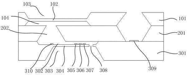
[0022] Such as figure 1 The shown MEMS sensor includes: a first substrate 101, a second substrate 201, and a third substrate 301 made of a single crystal silicon wafer. The third substrate 301 is the base of the MEMS micromechanical sensor, and the second substrate 201 is placed on the third substrate. The substrate 301 is above and connected to the third substrate 301 , the first substrate 101 is placed above the second substrate 201 and connected to the second substrate 201 .
[0023] The first substrate 101 is processed by the MEMS process to obtain a first cavity 103 with an upward opening and a second cavity 104 with a downward opening. The part of the first substrate between the first cavity 103 and the second cavity 104 constitutes the first film. sheet 102,
[0024] The second substrate 201 is provided with a first through hole 202 , and the first throug...
PUM
 Abstract
Description
Claims
Application Information
