Quad-core processor system built in quad-core structure and data switching method thereof
A nuclear processor and data exchange technology, applied in the direction of machine execution devices, concurrent instruction execution, etc., can solve the problems of energy consumption, high power consumption, lack of high performance, low power consumption, etc., to improve data exchange efficiency and improve execution Efficiency, the effect of exploiting parallelism
- Summary
- Abstract
- Description
- Claims
- Application Information
AI Technical Summary
Problems solved by technology
Method used
Image

Examples
Embodiment 1
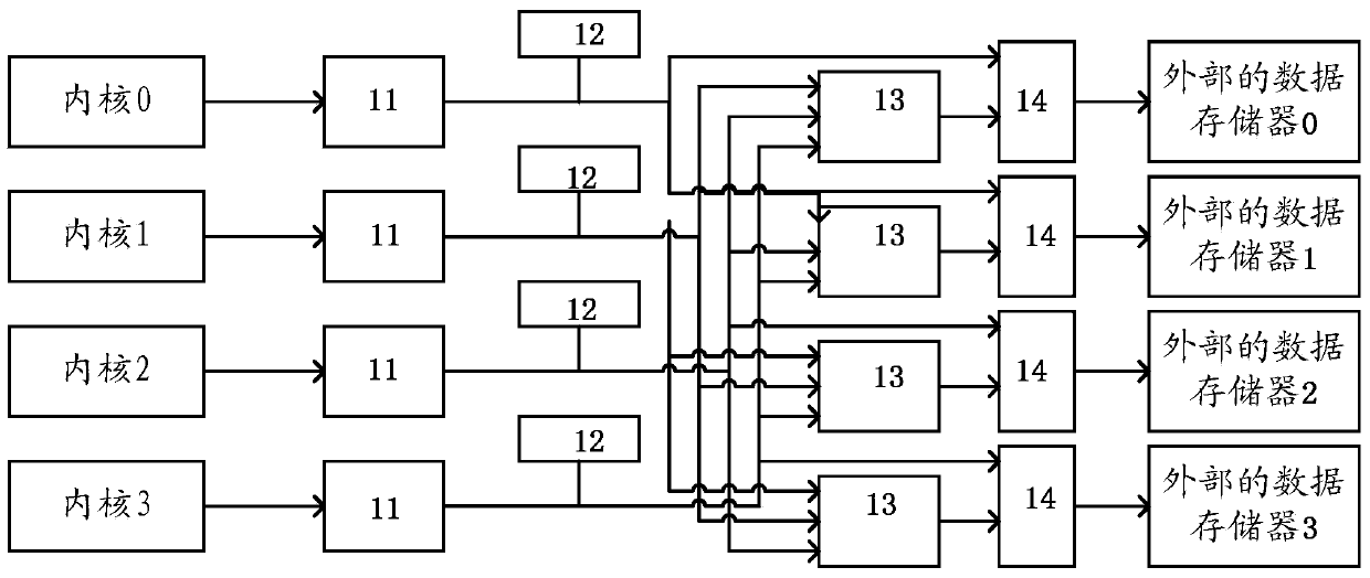
[0064] like figure 1 As shown, the present invention provides a quad-core processor system built with a quad-core structure, and processes data in a single program segment multi-data manner, that is, all microprocessor cores strictly execute the same program segment at the same time, and process multi-dimensional data in parallel. The system includes 4 RISC microprocessor cores, wherein,
[0065] Each microprocessor core includes:
[0066] an instruction memory for storing instructions;
[0067] In-kernel data memory for storing data;
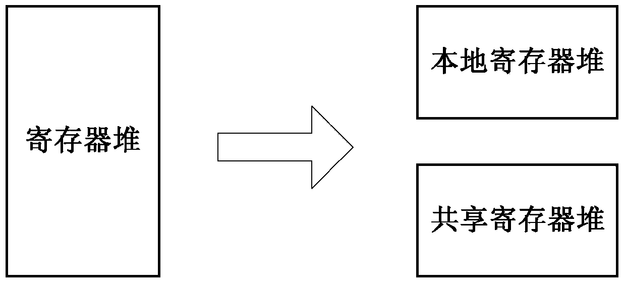
[0068] The central processing unit is used to perform corresponding operations according to the input instructions and data, and update the internal register file and the external data memory of the central processing unit.
[0069] Preferably, the central processing unit includes:
[0070] The fetching module is used to fetch instructions from the instruction memory according to the current pointer value in the current cycle, and calculate...
Embodiment 2
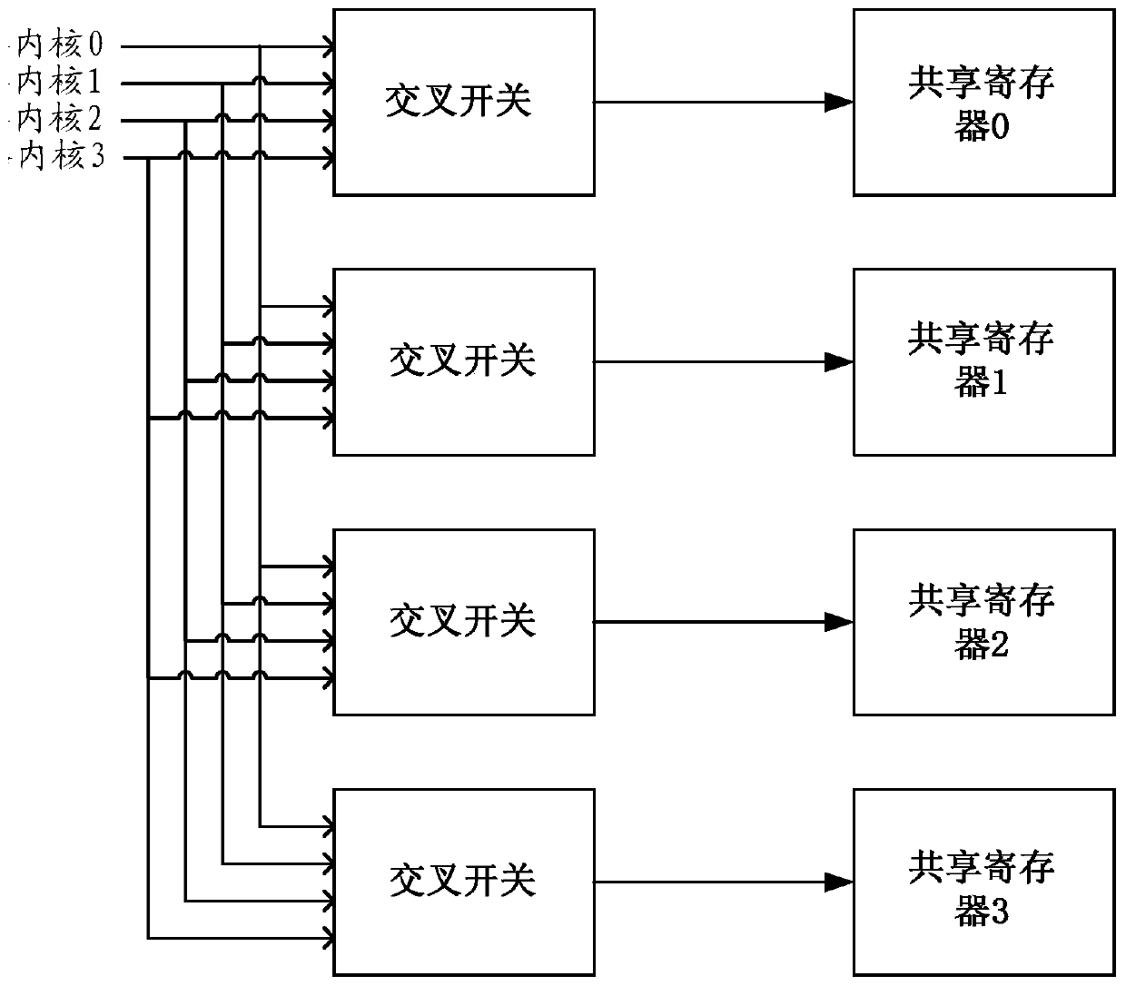
[0094] like Figure 5 As shown, the present invention also provides another data exchange method, using the quad-core processor system described in Embodiment 1, the method comprising:
[0095] Step S1, the configuration register of each microprocessor core is initialized according to the parallel code of a specific application, that is, the configuration register of each microprocessor core is configured according to the configuration instruction; specifically, the initialization is performed according to the parallel code of a specific application configuration register. That is, the configuration information is written to the configuration registers inside the four cores through configuration instructions;
[0096] Step S2, the data exchange between the external data memory and the microprocessor core, the initial data exchange is that the external data memory writes data to the register file of the microprocessor core, and there will be an external data memory and the mic...
PUM
 Abstract
Description
Claims
Application Information
 - R&D
- Intellectual Property
- Life Sciences
- Materials
- Tech Scout
- Unparalleled Data Quality
- Higher Quality Content
- 60% Fewer Hallucinations
Browse by: Latest US Patents, China's latest patents, Technical Efficacy Thesaurus, Application Domain, Technology Topic, Popular Technical Reports.
© 2025 PatSnap. All rights reserved.Legal|Privacy policy|Modern Slavery Act Transparency Statement|Sitemap|About US| Contact US: help@patsnap.com