Optical communication interconnection txv 3D integrated packaging and packaging method

An integrated packaging and optical communication technology, applied in the field of microelectronics, can solve the problems of limiting the operating frequency of electronic systems, affecting the mechanical strength and integration, and the proportion of through holes should not be too high, so as to reduce packaging costs, avoid electromagnetic signal interference, and improve The effect of substrate strength

Inactive Publication Date: 2016-08-17
INST OF ELECTRONICS ENG CHINA ACAD OF ENG PHYSICS
View PDF3 Cites 2 Cited by
  • Summary
  • Abstract
  • Description
  • Claims
  • Application Information

AI Technical Summary

Problems solved by technology

The through hole process in the current 3D integrated package is relatively complicated, and is limited by the metal hole filling process. The ratio of the depth to diameter of the through hole cannot be too high, so the problem is that the substrate should not be too thick and the hole should not be too small. , requires a thinning process, which affects the mechanical strength and integration
Even if some special technology can be used to achieve a relatively high aspect ratio of metal vias, the slender metal vias will also bring parasitic parameters such as inductance, which limits the increase in the operating frequency of electronic systems

Method used


Image

  • Optical communication interconnection txv 3D integrated packaging and packaging method
  • Optical communication interconnection txv 3D integrated packaging and packaging method
  • Optical communication interconnection txv 3D integrated packaging and packaging method

Examples


Embodiment

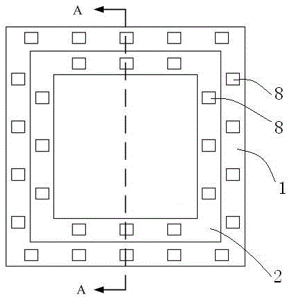
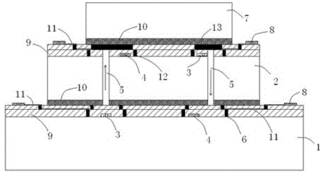
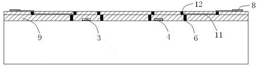
[0033] Such as Figure 1 to Figure 5 As shown, the optical communication interconnection TXV 3D integrated package includes a first chip 1, a second chip 2 bonded to the first chip, the first chip and the second chip both include an opaque substrate, and are deposited on A passivation layer 9 on an opaque substrate, a light-emitting device 3 and a photosensitive device 4 embedded in the passivation layer, a plurality of metal electrodes 8 for bonding external leads, and connecting with the metal electrodes to realize internal electrical signal interconnection The metal leads 11; the first chip also includes a metal hole 6 in the passivation layer to realize internal interconnection, and the second chip also includes a through hole 5 to realize the optical communication interconnection between the first chip and the second chip, The second metal layer 14 located at the bottom of the second chip for bonding the first chip and the second chip, the isolation metal pillar 12 embedd...


PUM


Abstract

The invention discloses an optical communication interconnection through-X-via (TXV) 3D integrated package and a packaging method, and solves the problems that a process is complicated, the integration level is low and the working frequency is limited in the prior art. The method comprises the following steps of a, manufacturing a chip with a through hole and a chip without a through hole; b, depositing a metal layer on a substrate such as glass or silicon, and patterning to obtain an optical path cover plate; c, aligning and bonding the optical path cover plate, the chip with the through hole and the chip without the through hole to complete 3D integrated package. By the method, through holes with a high aspect ratio can be obtained, procedures of thinning the chips, depositing a through hole dielectric layer and a seed layer, electroplating metal for filling holes and the like are not required, the integration level of the 3D integrated package can be greatly improved, the packaging cost is reduced, the problems of parasitic inductance, capacitance and signal coupling are solved and the working frequency of an electronic system can be greatly improved.

Description

technical field [0001] The invention belongs to the technical field of microelectronics, and in particular relates to an optical communication interconnection TXV 3D integrated package and a package method. Background technique [0002] With the development of microelectronic integrated circuit technology and people's requirements for electronic products in the direction of miniaturization and multi-function, integrated circuits and electronic systems require smaller and smaller volumes, higher integration and stronger functions. However, when circuit integration and packaging develop in a higher direction according to Moore's Law, its power consumption, heat dissipation, and cost have become serious constraints. Therefore, various new technologies, new materials, and new designs have been proposed to solve this problem. Among them, through-silicon via (TSV) 3D and through-glass via (TGV) 3D integrated packaging technologies are considered to be the most promising technical ...

Claims


Application Information

Patent Timeline
Patent Type & Authority Patents(China)
IPC IPC(8): H01L23/498H01L21/60
CPCH01L2924/0002
Inventor 唐海林熊永忠
Owner INST OF ELECTRONICS ENG CHINA ACAD OF ENG PHYSICS
Why Eureka
Try Eureka