Cache-on-board (COB) technology-based integrated light emitting diode (LED) packing method

A technology of LED packaging and LED chips, applied in the direction of electrical components, circuits, semiconductor devices, etc., can solve the problems of uncontrollable shape, position, quantity, and thickness of fluorescent glue, low packaging efficiency, poor product consistency, etc., to simplify LED The effects of integrated packaging procedures, lower product costs, and reduced waste

Inactive Publication Date: 2012-05-02
秦会斌 +6
View PDF2 Cites 4 Cited by
  • Summary
  • Abstract
  • Description
  • Claims
  • Application Information

AI Technical Summary

Problems solved by technology

However, with this method, the shape, position, quantity, and thickness of the fluorescent glue cannot be controlled, resulting in relatively low packaging efficiency and poor product consistency.

Method used


Image

  • Cache-on-board (COB) technology-based integrated light emitting diode (LED) packing method
  • Cache-on-board (COB) technology-based integrated light emitting diode (LED) packing method
  • Cache-on-board (COB) technology-based integrated light emitting diode (LED) packing method

Examples


Embodiment 1

[0027] An integrated LED packaging method based on COB technology, comprising the following steps:

[0028] 1) Adjust the thickness of the mold and the diameter of the reserved hole;

[0029] 2) Align the reserved hole on the mold with the LED chip on the aluminum-based circuit board that has been solidified, and cover the mold on the aluminum-based circuit board;

[0030] 3) Baking is performed after applying fluorescent glue, and the mold is removed after baking to obtain an LED packaging unit.

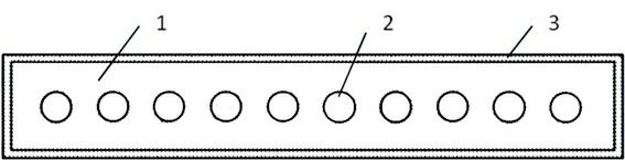
[0031] The mold in step 1 includes a substrate and reserved holes, the substrate is provided with a number of reserved holes, and flanges for positioning and fixing are provided around the back of the substrate.

[0032] The mold in step 1 is prepared from silicone rubber.

[0033] The upper and lower surfaces of the mold in step 1 are polygonal, circular or oval.

[0034] The baking temperature in step 3 is 140-160°C.

Embodiment 2

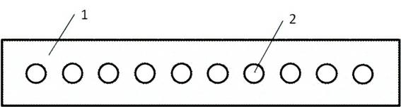
[0036] like figure 1 , 2 , 3, is a kind of dot fluorescent rubber mold, which is made of a silicone rubber plate 1 as a base material, and a flange 3 is processed during molding, and then a reserved hole 2 is processed on it according to the size of the LED package. The shape, position, thickness and quantity of the fluorescent glue can be adjusted by adjusting the thickness of the silicone rubber plate 1 and the diameter of the reserved hole 2, and the height of the flange 3 can be adjusted by the thickness of the aluminum-based circuit board

Embodiment 3

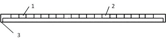
[0038] like Figure 4 As shown, the schematic diagram after direct bonding 5 on the aluminum-based circuit board 4 .


PUM


Abstract

The invention relates to a cashe-on-board (COB) technology-based integrated light emitting diode (LED) packing method, which comprises the following steps that: 1. thickness of a mould and diameter of a reserved hole are adjusted; 2. the reserved hole on the mould is aligned to an LED chip which is well fixed on an aluminum circuit board, and the mould covers the aluminum circuit board; 3. after fluorescent glue is sprayed on the aluminum circuit board, the aluminum circuit board is baked, then the mould is removed after the baking so as to obtain an LED packing unit. The method has followinng beneficial effects that: the shape, position, thickness and quantity of the fluorescent flue can be adjusted by adjusting the thickness of a silicone board and the diameter of the reserved hole, so the LED integrated packing procedures can be simplified, the heat resistance and the working temperature of the LED chip can be reduced, the shape, position, thickness and quantity of the fluorescent glue can be flexible to control, the light emitting efficiency and the consistency, stability and service life of the product can be improved, the packing efficiency also can be improved, the waste can be reduced, and the product cost can be reduced. The baking temperature is set as 140 to 160 DEG C, so the packing effect is better.

Description

technical field [0001] The invention designs an integrated LED packaging method based on COB technology, and in particular relates to an integrated LED packaging method based on COB technology in the field of LED packaging. technical background [0002] With the continuous development of semiconductor lighting technology, the application field of LED is also expanding, gradually spreading from outdoor lighting to indoor lighting, while fluorescent lamps and ceiling lamps are the mainstream products of indoor lighting. The packaging of the LED circuit boards of existing LED fluorescent lamps and ceiling lamps mostly adopts pre-packaged single LED light sources, which are welded on aluminum-based circuit boards for circuit connection and heat dissipation. This connection method leads to an increase in the number of heat transfer layers and an extension of the path between the LED chip and the aluminum-based circuit board, thereby greatly reducing the speed at which the heat ge...

Claims


Application Information

Patent Timeline
Patent Type & Authority Applications(China)
IPC IPC(8): H01L33/48H01L33/50
Inventor 秦会斌丁申冬郑鹏秦惠民祁姝琪许振军夏琦
Owner 秦会斌
Why Eureka
Try Eureka