Quantum-dot light emitting diode (QLED) device and fabrication method thereof

A device, high thermal conductivity technology, applied in semiconductor devices, electrical components, circuits, etc., can solve the problems affecting the heat dissipation efficiency and working life of QLED devices, and the poor heat dissipation effect of isolated bank materials, so as to improve the life, long working life, Slow down the effect of decay

Active Publication Date: 2017-06-20
TCL CORPORATION
View PDF9 Cites 27 Cited by
  • Summary
  • Abstract
  • Description
  • Claims
  • Application Information

AI Technical Summary

Problems solved by technology

[0005] The purpose of the present invention is to provide a QLED device and a preparation method thereof, aiming to solve the problem that the heat dissipation efficiency and working life of the QLED device are affected due to the poor heat dissipation effect of the isolation bank material in the existing QLED device

Method used


Image

  • Quantum-dot light emitting diode (QLED) device and fabrication method thereof
  • Quantum-dot light emitting diode (QLED) device and fabrication method thereof
  • Quantum-dot light emitting diode (QLED) device and fabrication method thereof

Examples


Embodiment Construction

[0016] In order to make the technical problems, technical solutions and beneficial effects to be solved by the present invention clearer, the present invention will be further described in detail below in conjunction with the embodiments. It should be understood that the specific embodiments described here are only used to explain the present invention, not to limit the present invention.

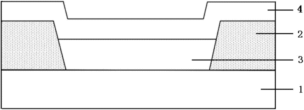
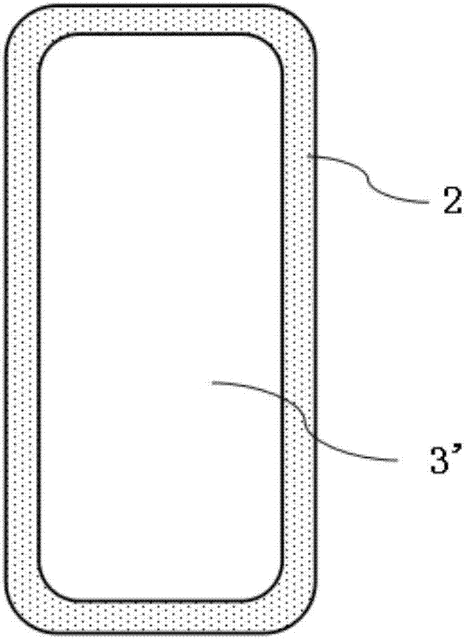
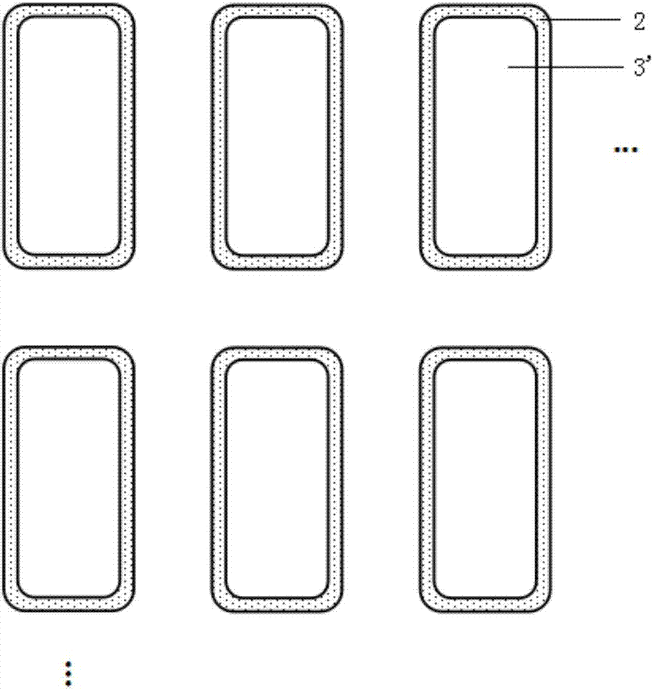
[0017] combine Figure 1-Figure 3 , an embodiment of the present invention provides a QLED device, including a first electrode 1, an isolation bank 2 for defining a pixel area 3', an optical layer 3 disposed on the pixel area 3', and an isolation bank 2 covering the and the second electrode 4 of the optical layer 3, wherein the isolation bank 2 contains a high thermal conductivity material, and the thermal conductivity of the high thermal conductivity material is ≥ 10WK -1 m -1 .

[0018] Such as figure 1 As shown, a schematic longitudinal cross-sectional view of the QLED device describ...


PUM


Abstract

The invention provides a quantum-dot light emitting diode (QLED) device. The QLED device comprises a first electrode, an isolation bank, an optical layer and a second electrode, wherein the isolation bank is used for defining a pixel region, the optical layer is arranged in the pixel region, the second electrode covers the isolation bank and the optical layer, the isolation bank contains a high thermal conduction material, and the thermal conductivity of the high thermal conduction material is more than or equal to 10WK<-1>m<-1>. A fabrication method of the QLED device comprises the following steps of providing the first electrode; depositing a bank material layer on a surface of the first electrode, wherein the bank material layer contains the high thermal conduction material, and the thermal conductivity of the high thermal conduction material is more than or equal to 10WK<-1>m<-1>; sequentially performing photoetching, polishing and surface processing on the bank material layer to obtain the isolation bank for defining the pixel region; and depositing the optical layer in the pixel region, wherein the second electrode covers the surfaces of the isolation bank and the optical layer.

Description

technical field [0001] The invention belongs to the field of display technology, and in particular relates to a QLED device and a preparation method thereof. Background technique [0002] Inorganic nanocrystalline quantum dot luminescent materials not only have the advantages of saturated color of emitted light and adjustable wavelength, but also have high photoluminescence and electroluminescence quantum yields, which are suitable for the preparation of high-performance display devices. In addition, from the perspective of preparation technology, quantum dot luminescent materials can be prepared into films by spin coating, printing, printing equipment and other solution processing methods under non-vacuum conditions. Therefore, quantum dot light-emitting diodes (QLEDs) prepared with quantum dot films have become a strong competitor for next-generation display technologies. [0003] Generally, a QLED device includes a first electrode, a hole injection layer, a hole transpor...

Claims


Application Information

Patent Timeline
Patent Type & Authority Applications(China)
IPC IPC(8): H01L33/64H01L33/04H01L33/00
CPCH01L33/005H01L33/04H01L33/641
Inventor 陈崧钱磊杨一行曹蔚然向超宇
Owner TCL CORPORATION
Why Eureka
Try Eureka