

Array substrate and display device
A technology of array substrate and display device, applied in nonlinear optics, instruments, optics, etc., can solve the problem of low utilization rate of light energy, and achieve the effect of improving utilization rate of light energy
- Summary
- Abstract
- Description
- Claims
- Application Information
AI Technical Summary
Problems solved by technology
Method used
Image

Examples
Embodiment 1
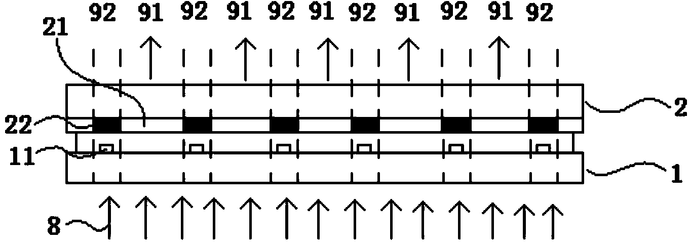
[0025] Such as image 3 As shown, the present embodiment provides an array substrate 1 and a display device having the array substrate 1 .
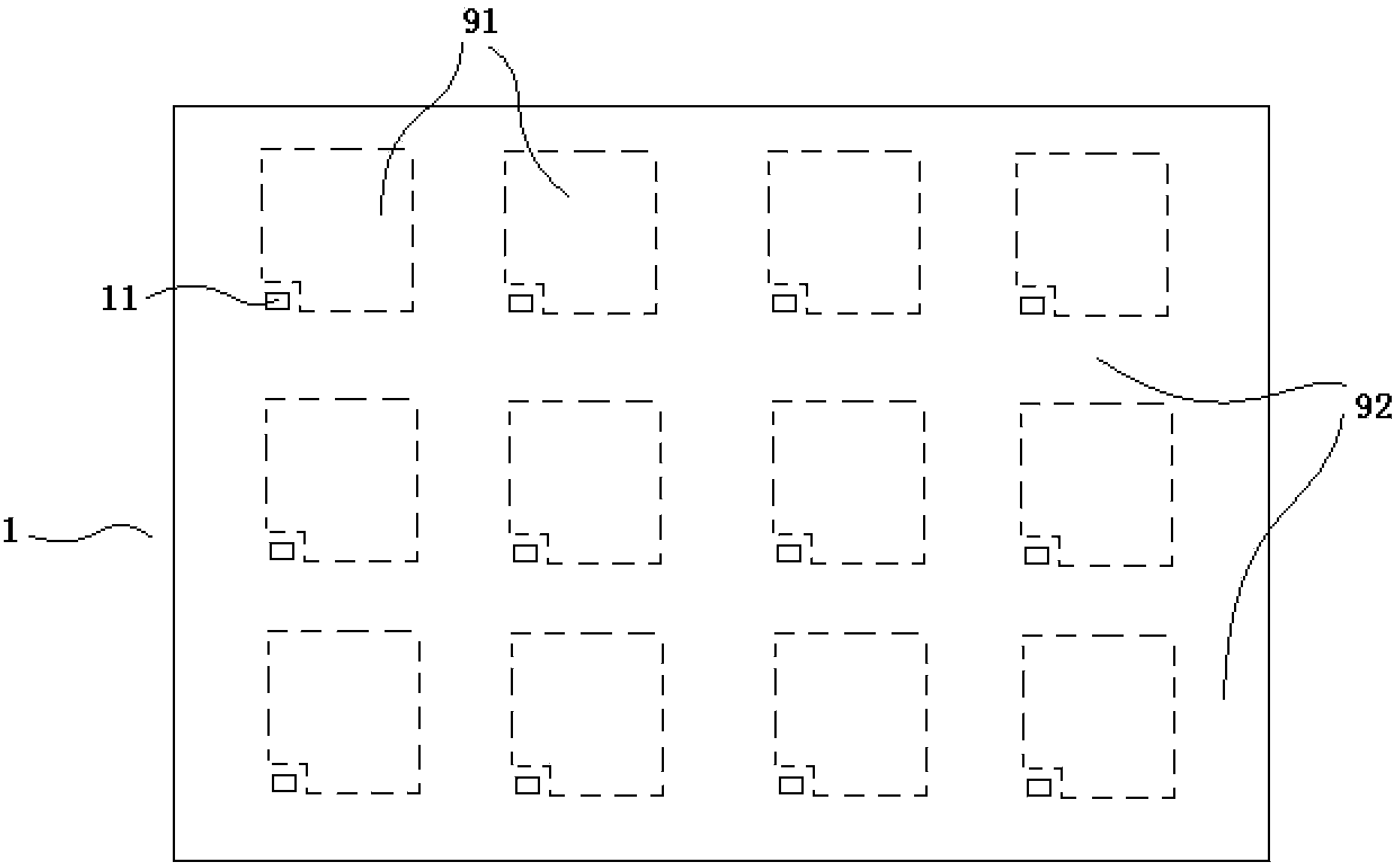
[0026] The array substrate 1 of this embodiment includes a plurality of light-transmitting regions 91 arranged at intervals for displaying, and a light-shielding region 92 surrounding each light-transmitting region 91 . Wherein, generally, each light-transmitting area 91 corresponds to a pixel unit, and the light-transmitting area 91 is the area where the pixel electrodes of each pixel unit are located, so that a specific electric field can be formed in the light-transmitting area 91 to display desired content. The light-shielding area 92 is an area located outside each light-transmitting area 91, where other display structures such as gate lines, data lines, and thin-film transistors 11 are arranged. Since these display structures cannot form a correct electric field for display, The light at these positions should be blocked and not em...
Embodiment 2
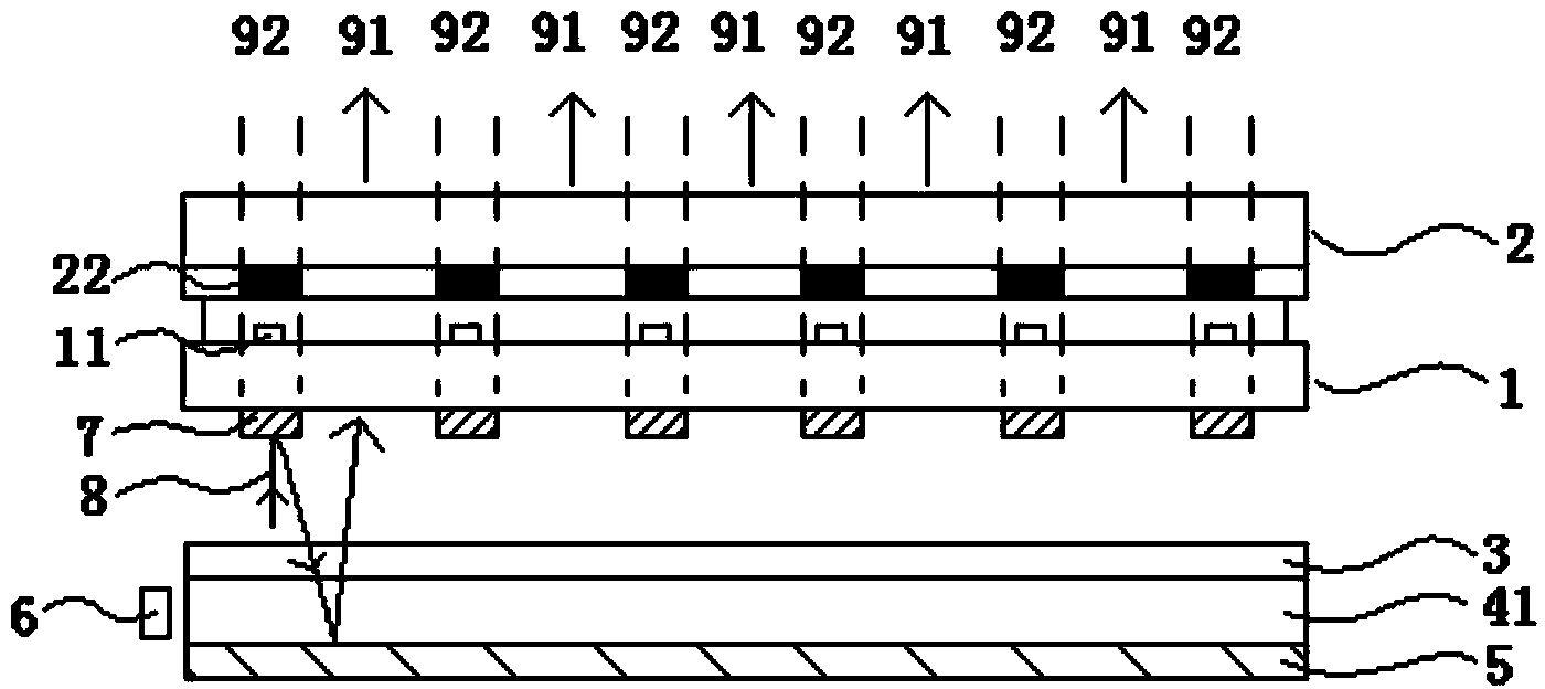
[0040] Such as Figure 4 As shown, this embodiment provides a display device, which includes a display panel and a backlight module for emitting light to the display panel. The backlight module includes a light source 6 and a reflective film for reflecting light from the light source 6 to the display panel. Layer 5.
[0041]The display device further includes a reflective layer 7 disposed at a position corresponding to the light-shielding area 92 of the display panel, which is used to reflect light from the light source 6 to the reflective film layer 5 .
[0042] That is to say, similar to Embodiment 1, the display device of this embodiment also includes a reflective layer 7, but the reflective layer 7 is not limited to be located in the array substrate 1, and it can also be located in other positions, as long as it can shield light from the light. The light in the region 92 is reflected back to the reflective film layer 5 for reuse.
[0043] Specifically, such as Figure 4...
Embodiment 3
[0048] Such as Figure 5 As shown, this embodiment provides a display device, the structure of which is similar to that of the display device in Embodiment 2.
[0049] The difference between the display device of this embodiment and the display device of Embodiment 2 is that the backlight module of the display device of this embodiment is a direct type backlight module.
[0050] Such as Figure 5 As shown, the direct type backlight module includes a diffusion plate 42, the diffusion plate 42 includes a light incident surface and a light output surface opposite, the reflective film layer 5 is arranged outside the light incident surface of the diffusion plate 42, and the light source 6 is arranged on the light incident surface of the diffusion plate 42 Between the reflective film layer 5 and the light-emitting surface of the diffusion plate 42, an optical film layer 3 is provided.
[0051] Preferably, the reflective layer 7 is disposed on the light-emitting surface of the diff...
PUM
 Abstract
Description
Claims
Application Information