Eureka AIR delivers breakthrough ideas for toughest innovation challenges, trusted by R&D personnel around the world.

Chip packaging method and structure

A chip packaging structure and chip packaging technology, applied in the direction of semiconductor/solid-state device parts, semiconductor devices, electrical components, etc., can solve the problems of poor reliability of chip packaging methods, and achieve the effect of simplifying the process

Active Publication Date: 2014-04-30
CHINA WAFER LEVEL CSP
View PDF8 Cites 11 Cited by
  • Summary
  • Abstract
  • Description
  • Claims
  • Application Information

AI Technical Summary

Problems solved by technology

[0005] The problem solved by the invention is that the reliability of the prior art chip packaging method is poor

Method used


Image

  • Chip packaging method and structure
  • Chip packaging method and structure
  • Chip packaging method and structure

Examples


Embodiment Construction

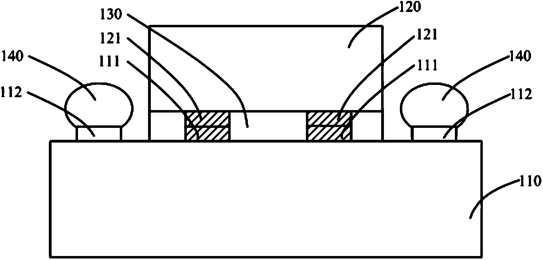
[0035] Usually, when two chips of different sizes are packaged in a system-in-package, the connection area between the big chip and the small chip is only the size of the small chip. Please refer to figure 1 , figure 1 It is a schematic cross-sectional structure schematic diagram of system-in-package for two chips with different sizes in the prior art, including: a first chip 110, the surface of the first chip 110 has a first pad 111 and a third pad 112; Chip 120, the area of ​​the second chip 120 is smaller than the first chip 110, the surface of the second chip 120 has a second pad 121, the second pad 121 on the surface of the second chip 120 is connected to the The first pads 111 on the surface of the first chip 110 are correspondingly bonded together; the insulating glue 130 is located in the gap between the surface of the first chip 110 and the surface of the second chip 120, and is used to bond the first chip 110 and the second chip 120; solder balls 140, located on th...


PUM


Abstract

The invention provides a chip packaging method and structure. The chip packaging method includes the first step of providing a first chip, wherein the surface of the first chip is provided with a plurality of first bonding pads, the second step of providing a second chip, wherein the surface of the second chip is provided with a plurality of second bonding pads, the second bonding pads correspond to the first bonding pad in position, and the area of the second chip is smaller than that of the first chip, the third step of correspondingly combining the second bonding pads on the surface of the second chip and the first bonding pads on the surface of the first chip, and the fourth step of forming a first insulation layer, wherein the first insulation layer is coated on the second chip and combined with the first chip. The chip packaging method improves reliability of the packaging structure.

Description

technical field [0001] The invention relates to the technical field of semiconductors, in particular to a chip packaging method and structure. Background technique [0002] With the continuous progress of semiconductor chip manufacturing, integration and packaging technology, electronic systems gradually show the development trend of multi-function, high performance and high reliability. In order to combine multiple active and passive components with different functions, as well as other components such as MEMS and Optics components in the same package, making it a system that can provide multiple functions Or subsystems, the industry has proposed system-in-package technology. [0003] The system-in-package can be used as a standard unit for PCB assembly, or it can be the final electronic product. Different from traditional chip packaging, system-in-package can be applied not only to digital systems, but also to optical communication, sensors, MEMS and other fields. Theref...

Claims


Application Information

Patent Timeline
IPC IPC(8): H01L21/60H01L23/498H01L23/488H01L25/16
CPCH01L2224/73204H01L24/09H01L24/14H01L24/73H01L24/81H01L2924/1461H01L2224/16145H01L2224/1703H01L2224/171H01L2924/00
Inventor 李俊杰王之奇杨莹喻琼祁俊华张坚王蔚
Owner CHINA WAFER LEVEL CSP
Why Eureka
Eureka Blog
Learn More