Switching power supply driving circuit and dead time adjusting method thereof
A driving circuit, switching power supply technology, applied in electrical components, output power conversion devices, AC power input conversion to DC power output and other directions, can solve the problem of bombing, low efficiency, and poor adjustment of the dead time of the upper and lower FETs. And other issues
- Summary
- Abstract
- Description
- Claims
- Application Information
AI Technical Summary
Problems solved by technology
Method used
Image
Examples
Embodiment Construction
[0017] The technical solutions of the present invention will be described in further detail below in conjunction with the accompanying drawings.
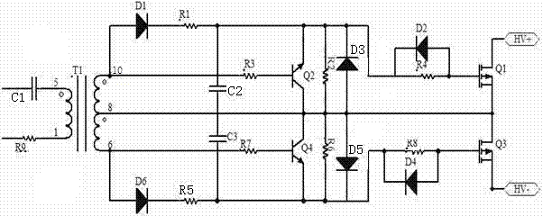
[0018] Such as figure 2 As shown, a switching power supply driving circuit includes a first input terminal, a second input terminal, a transformer T1, a first capacitor C1, and first to ninth resistors (R1, R2, R3, R4, R5, R6, R7, R8, R9), first to sixth diodes (D1, D2, D3, D4, D5, D6), first triode Q2, second triode Q4, first field effect transistor Q1, second Field effect transistor Q3, positive output terminal HV+ and negative output terminal HV-, transformer T1 includes a primary side and two secondary sides, and the two secondary sides have a common output terminal 8; the first input terminal is connected to the primary side through C1 One terminal 5, the second input terminal is connected to the other terminal 1 of the primary side through R9; the other output terminal 10 of the first secondary side is connected to the anode...
PUM
 Abstract
Description
Claims
Application Information


