Clamp for sputtering and method for sputtering semiconductor package

A technology for semiconductors and packages, which is applied in the field of sputtering fixtures and semiconductor packages for sputtering, and can solve problems such as defective products and easy overflow plating

Active Publication Date: 2014-05-21
SILICONWARE PRECISION IND CO LTD
View PDF10 Cites 5 Cited by
  • Summary
  • Abstract
  • Description
  • Claims
  • Application Information

AI Technical Summary

Problems solved by technology

[0004] like figure 1 As shown, it provides a carrier plate 10 with an electrostatic chuck 101 in the plasma processing chamber 15, and the electrostatic chuck 101 fixes the semiconductor package 11 on the carrier plate 10 by electrostatic clamping force, and on the carrier plate 10 An electrode 13 is provided above the semiconductor package 11, and a plasma region 14 is formed between the semiconductor package 11 and the electrode 13, and the gas in the plasma region 14 is excited by radio frequency (RF) to generate plasma for sputtering, And sputtering this semiconductor package 11, yet, aforesaid sputtering method easily overflows to the bottom surface 112 of this semiconductor package 11, causes the generation of defective product

Method used


Image

  • Clamp for sputtering and method for sputtering semiconductor package
  • Clamp for sputtering and method for sputtering semiconductor package
  • Clamp for sputtering and method for sputtering semiconductor package

Examples


no. 1 example

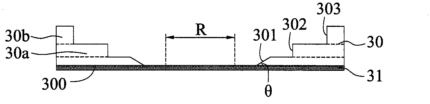
[0051] Such as Figure 3A to Figure 3E What is shown is a schematic cross-sectional view of the first embodiment of the method for sputtering a semiconductor package and the jig used for the sputtering process of the present invention.

[0052] Such as Figure 3A As shown, a fixture plate 30 is provided, which has a first opening 301 passing through the fixture plate 30, and the cross section of the first opening 301 of the fixture plate 30 is tapered with a narrow bottom and a wide top, and the first The range of the angle θ between the conical slope of the opening 301 and the bottom surface of the jig plate 30 is preferably between 10° and 90°, and the jig plate 30 also includes a first stepped layer 30a and a second stepped layer 30b, the first stepped layer 30a is arranged on the top surface of the jig plate 30, and has a second opening 302 correspondingly exposing the first opening 301, in addition, the second stepped layer 30b is arranged on the first stepped layer 30a ...

no. 2 example

[0057] Figure 4 It is a schematic cross-sectional view of the second embodiment of the method for sputtering a semiconductor package and the jig used for the sputtering process of the present invention.

[0058] This embodiment is substantially the same as the first embodiment, the main difference is that the jig plate 35 of this embodiment does not have the first stepped layer 30a and the second stepped layer 30b, and the top surface 322 of the semiconductor package 32 It is flush with the top surface 352 of the jig plate 35 .

no. 3 example

[0060] Figure 5 It is a schematic cross-sectional view of a third embodiment of the method for sputtering a semiconductor package and the jig used for the sputtering process according to the present invention.

[0061] This embodiment is substantially the same as the second embodiment, the main difference being that the top surface 361 of the semiconductor package 36 in this embodiment is higher than the top surface 352 of the fixture board 35 .


PUM


Abstract

The invention provides a clamp for sputtering and a method for sputtering a semiconductor package. The clamp comprises a bearing plate having a groove, an adhering layer disposed at the bottom face of the groove and provided with an object setting area at the top face, and a jig plate which is combined with the adhering layer and is embedded in the groove of the bearing plate and is provided with a first opening corresponding to the object setting area. The cross section of the first opening of the jig plate is in the shape of an oval, which is narrow at bottom and wide at top, and a predetermined distance is disposed between the edge of the object setting area and the bottom end of the first opening. Accordingly, the bottom part of the semiconductor package can be prevented from sputtering, and the yield of the semiconductor packages can be increased.

Description

technical field [0001] The invention relates to a jig structure and a method for manufacturing a semiconductor package, in particular to a jig used in a sputtering process and a method for sputtering a semiconductor package. Background technique [0002] A general semiconductor package is manufactured by electrically connecting a semiconductor chip to a carrier such as a lead frame or a package substrate, and then covering the semiconductor chip with an encapsulant on the carrier to prevent the semiconductor chip from being exposed to the outside atmosphere. contact, and thus protect against moisture or pollutants. However, when the semiconductor package is in operation, it will suffer from external electromagnetic interference (EMI) to some extent, which will cause the electrical operation function of the semiconductor package to be abnormal, thus affecting the overall electrical performance of the semiconductor package. . In view of the aforementioned EMI problems, metal...

Claims


Application Information

Patent Timeline
Patent Type & Authority Applications(China)
IPC IPC(8): C23C14/34
Inventor 张卓兴简俊忠许聪贤黄添崇赖文德
Owner SILICONWARE PRECISION IND CO LTD
Why Eureka
Try Eureka