
A stt-mram cache design method

A design method and cache technology, applied in computing, energy-saving computing, information storage, etc., can solve problems such as difficult universal and effective solutions, increase the static power consumption of the chip, and different memory access behaviors, and improve the performance of the chip. rate, reduce write power consumption, and improve performance

Active Publication Date: 2016-08-17
BEIHANG UNIV
View PDF3 Cites 0 Cited by
  • Summary
  • Abstract
  • Description
  • Claims
  • Application Information

AI Technical Summary

Problems solved by technology

[0009] First, the production processes of SRAM and STT-MRAM are different, and integrating them on the same chip will reduce the chip yield and increase production costs;
[0010] Second, the existence of SRAM will increase the static power consumption of the chip;
[0011] Third, how to determine the respective capacities of STT-MRAM and SRAM is also a difficult problem to solve, because different applications and programs have different memory access behaviors, so it is difficult to have a universally effective solution

Method used


Image

  • A stt-mram cache design method
  • A stt-mram cache design method
  • A stt-mram cache design method

Examples


Embodiment Construction

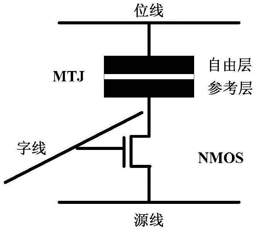
[0028] The working principle of the STT-MRAM storage unit involved in the present invention is as follows figure 1 shown. STT-MRAM memory cells generally adopt 1T1J (1Transistor and 1MTJ). Transistors control access to MTJ data. The structure of MTJ is divided into free layer, reference layer and intermediate oxide layer. Wherein the magnetization direction of the reference layer is fixed. By applying currents in different directions to the MTJ, the magnetization direction of the free layer can be changed. If the magnetization direction of the free layer is the same as that of the reference layer, the resistance value of the MTJ becomes smaller, and it can be regarded as storing logic "0". Otherwise, a logic "1" is stored. When reading the data of the memory cell, the word line is set to be valid, and a small voltage of 0.1V is applied between the bit line BL and the source line SL. According to the similarities and differences of the magnetization directions of the free ...


PUM


Abstract

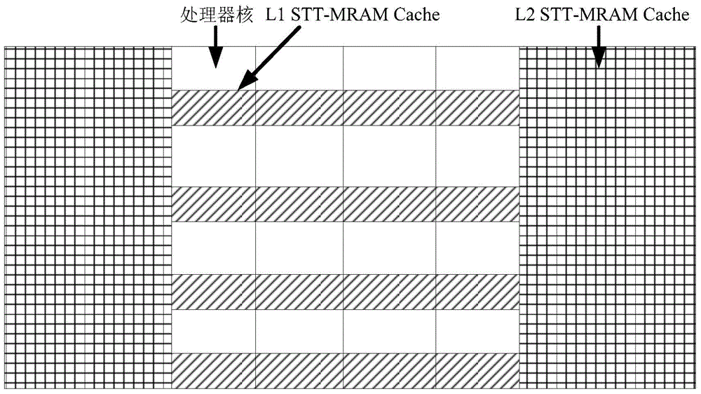
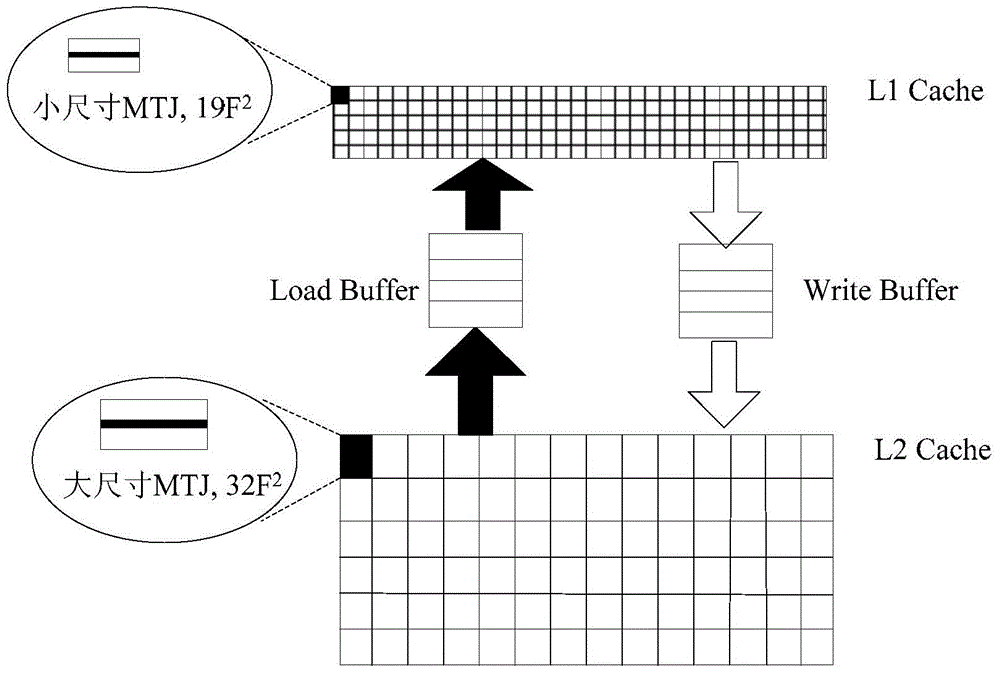
A novel STT-MRAM cache design method includes the three major steps. The relation among the size of MTJ, write currents and write energy consumption is utilized, a novel STT-MRAM cache structure is designed, and an L1Cache and an L2Cache are achieved through MTJ memory units with different sizes respectively. Compared with the mode that MTJ memory units only with the same size are used, write energy consumption is reduced, and performance is improved. Compared with the structure that an SRAM and an STT-MRAM are mixed, static power consumption is remarkably reduced. Due to the fact that the L1Cache is composed of the MTJ memory units with the small size, the L1Cache is smaller in size and higher in memory density, the miss rate of the Cache is remarkably lower than that of an SRAM Cache, and the memory access performance is improved. In addition, only the STT-MRAM production process is adopted, the yield of chips is increased, and production cost is reduced.

Description

technical field [0001] The present invention uses STT-MRAM storage devices to replace traditional SRAM devices as the cache memory of the chip, and proposes an STT-MRAM cache (Cache) design method, which reduces chip power consumption and improves chip performance. The invention belongs to the technical field of nonvolatile memory design. Background technique [0002] With the continuous improvement of on-chip transistor integration density, multi-core processors have begun to be widely used. For example, IBM Power7, Intel's Core series processors and Tilera's Tile-GX series processors. Although the multi-core processor greatly improves the performance of the computer, it needs the support of large-capacity on-chip cache to solve the "memory wall" bottleneck. At present, random static memory (SRAM) is widely used in the industry as an on-chip cache (Cache). To reduce processor power consumption, the on-chip supply voltage is continuously reduced. The subthreshold leakage...

Claims


Application Information

Patent Timeline
Patent Type & Authority Patents(China)
IPC IPC(8): G06F12/0893G11C11/16
CPCG06F12/0897G11C11/1673G11C11/1675Y02D10/00
Inventor 成元庆郭玮赵巍胜张有光
Owner BEIHANG UNIV
Learn More