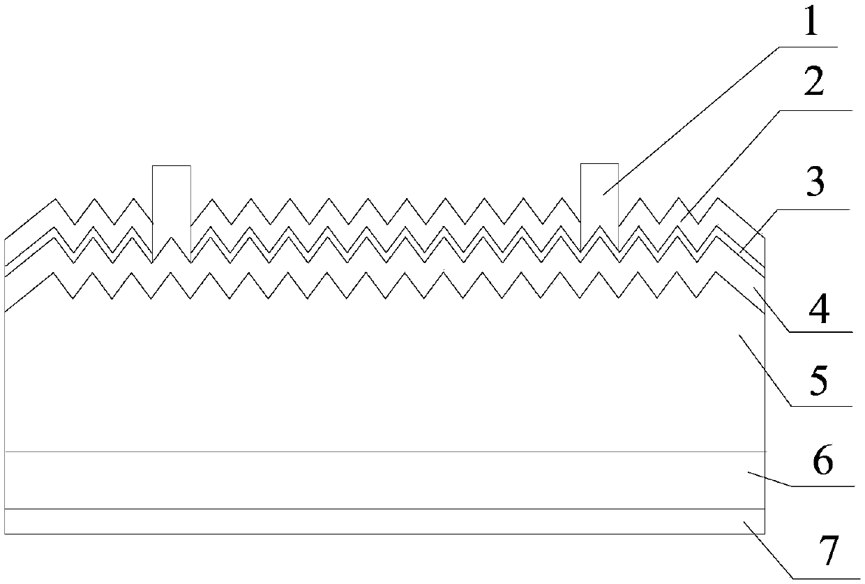
A method for making crystalline silicon solar cells by inkjet printing
An inkjet printing, solar cell technology, applied in the direction of copying/marking methods, printing, circuits, etc., can solve the problems of limited printing accuracy, depression, high conductivity, etc., to achieve good uniformity and repeatability, and uniformity between sheets Good, high print resolution results
- Summary
- Abstract
- Description
- Claims
- Application Information
AI Technical Summary
Problems solved by technology
Method used
Image
Examples
Embodiment 1
[0036] A method for making crystalline silicon solar cells by inkjet printing, comprising the following steps:
[0037] (1) Cleaning the surface of the P-type monocrystalline silicon wafer and making the textured surface is a surface formed by a pyramid, an inverted pyramid or a pit-like structure with a size of 0.1 to 100 microns;
[0038] (2) performing phosphorus doping on one side of the P-type monocrystalline silicon wafer after texturing to form a PN junction;
[0039] (3) Continue to deposit a layer of passivation and anti-reflection film on the N-type surface;
[0040] (4) Use inkjet printing to achieve surface metallization. Inkjet printing uses the piezoelectric effect of piezoelectric ceramics to make small ink droplets spray onto the surface of the silicon wafer through the nozzle. The diameter of the ink droplet is 30nm. The specific steps are as follows: first Spray printing 20 layers of sub grid line seed layer, and then spray print 50 layers of sub grid line c...
Embodiment 2
[0049] A method for making crystalline silicon solar cells by inkjet printing, comprising the following steps:
[0050] (1) Cleaning the surface of the P-type monocrystalline silicon wafer and making the textured surface is a surface formed by a pyramid, an inverted pyramid or a pit-like structure with a size of 0.1 to 100 microns;
[0051] (2) performing phosphorus doping on one side of the P-type monocrystalline silicon wafer after texturing to form a PN junction;
[0052] (3) Continue to deposit a layer of passivation and anti-reflection film on the N-type surface;
[0053] (4) Inkjet printing is used to achieve surface metallization, and the piezoelectric effect of piezoelectric ceramics is used to spray silver ink onto the surface of the silicon wafer through the nozzle. The diameter of the ink droplet is 20nm. 10 layers of wire seed layer, and then 40 layers of conductive layer for sub-grid lines; then 1 layer of seed layer for busbar lines, and finally 1 layer of condu...
Embodiment 3
[0056] A method for making crystalline silicon solar cells by inkjet printing, comprising the following steps:
[0057] (1) Cleaning the surface of the P-type monocrystalline silicon wafer and making the textured surface is a surface formed by a pyramid, an inverted pyramid or a pit-like structure with a size of 0.1 to 100 microns;
[0058] (2) performing phosphorus doping on one side of the P-type monocrystalline silicon wafer after texturing to form a PN junction;
[0059] (3) Continue to deposit a layer of passivation and anti-reflection film on the N-type surface;
[0060] (4) Inkjet printing is used to achieve surface metallization, and the piezoelectric effect of piezoelectric ceramics is used to spray silver ink onto the surface of the silicon wafer through the nozzle. The diameter of the ink droplet is 40nm. 50 layers of wire seed layer, and then 60 layers of conductive layer for sub-grid lines; then 10 layers of seed layer for busbar lines, and finally 10 layers of c...
PUM
| Property | Measurement | Unit |
|---|---|---|
| diameter | aaaaa | aaaaa |
| size | aaaaa | aaaaa |
| width | aaaaa | aaaaa |
Abstract
Description
Claims
Application Information
