

Manufacturing method of semiconductor device test sample
A manufacturing method and semiconductor technology, applied in the semiconductor field, can solve problems such as batch wafer defects, and achieve the effect of increasing the rate
- Summary
- Abstract
- Description
- Claims
- Application Information
AI Technical Summary
Problems solved by technology
Method used
Image

Examples
Embodiment Construction
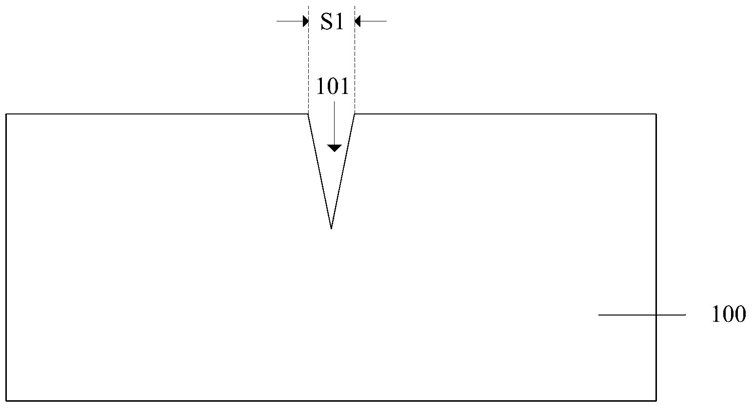
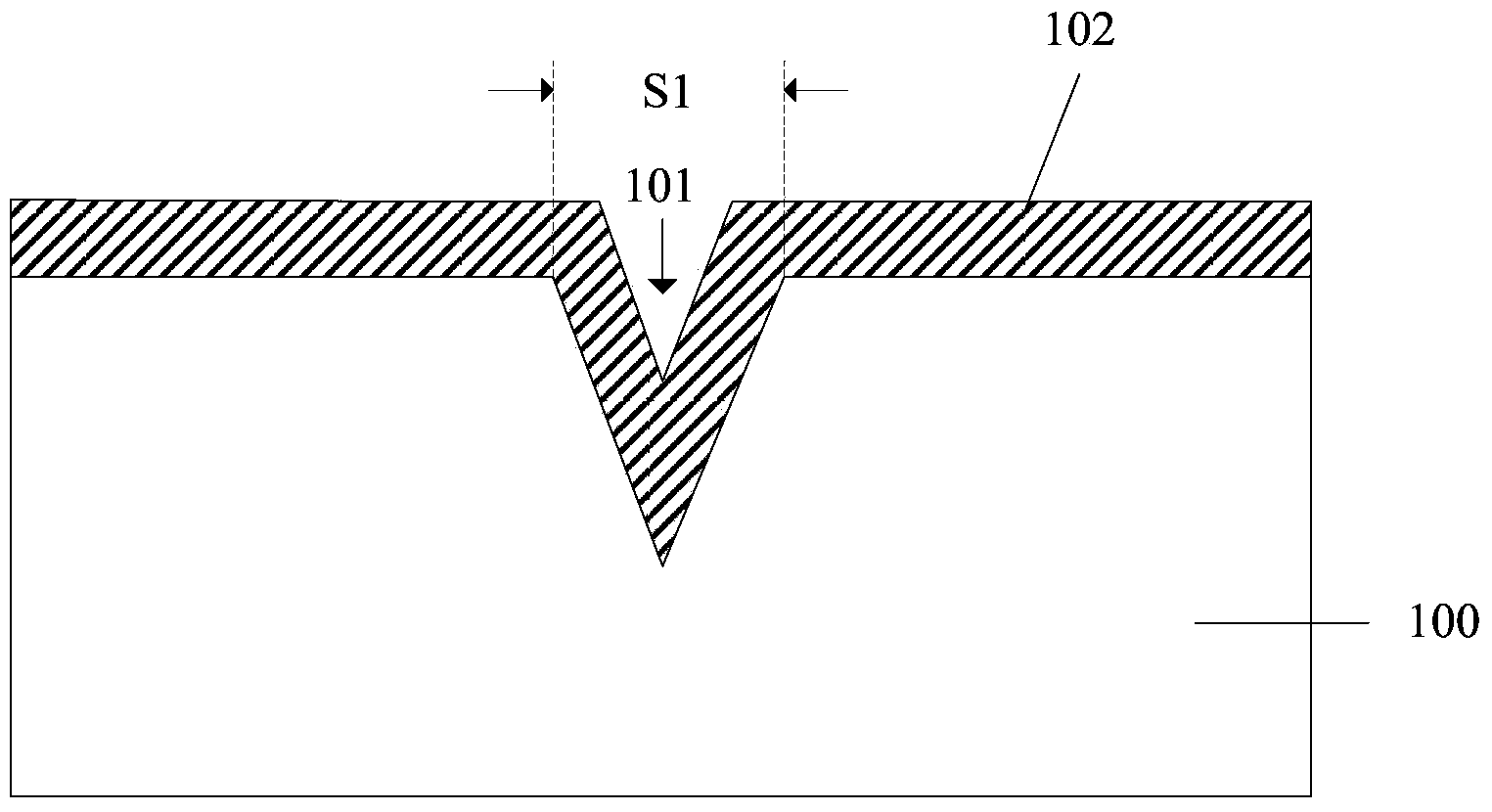
[0023] In the existing manufacturing process of semiconductor devices, defects such as dents with small sizes often occur. In the detection of defects such as dents with small sizes, it is difficult for the detection equipment to capture the defects, which is easy to cause batch failure. Wafers are scrapped due to defects, resulting in losses.
[0024] In order to solve the above-mentioned technical problems, the present invention provides a method for manufacturing test samples of semiconductor devices, so that wafer inspection equipment can more sensitively capture defects such as dents with smaller sizes, and monitor such defects in time to reduce Probability of failure of small semiconductor devices.
[0025] The detection method of semiconductor device defect of the present invention roughly comprises the following steps:
[0026] Provide a substrate; perform at least one oxidation treatment on the substrate, the oxidation treatment includes the steps of forming an oxide...
PUM
| Property | Measurement | Unit |
|---|---|---|
| Thickness | aaaaa | aaaaa |
Abstract
Description
Claims
Application Information