Semiconductor equipment machine quality monitoring method and system

A quality monitoring and semiconductor technology, applied in general control systems, control/regulation systems, computer control, etc., can solve the problems of manual calculation and input prone to errors, untimely, incomplete data, etc., to eliminate errors and improve product quality. Accurate and complete effect of rate and data

Active Publication Date: 2014-05-28
CSMC TECH FAB2 CO LTD
View PDF5 Cites 6 Cited by
  • Summary
  • Abstract
  • Description
  • Claims
  • Application Information

AI Technical Summary

Problems solved by technology

In the prior art, the quality monitoring of semiconductor equipment uses manual data recording, the recorded data is incomplete and not timely, and manual calculation and input are prone to errors

Method used


Image

  • Semiconductor equipment machine quality monitoring method and system
  • Semiconductor equipment machine quality monitoring method and system
  • Semiconductor equipment machine quality monitoring method and system

Examples


Embodiment Construction

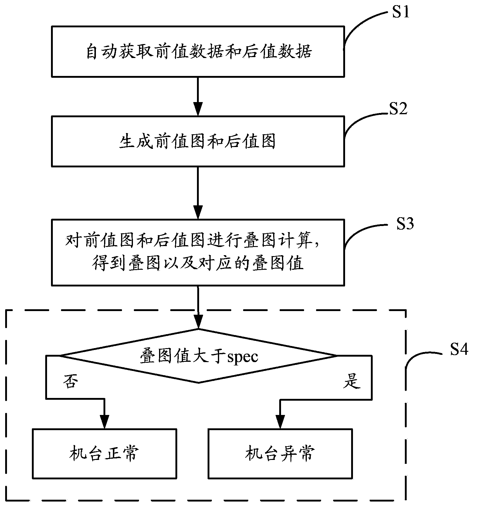
[0035] The invention discloses a method for monitoring the quality of a semiconductor equipment machine, the method comprising:

[0036] S1. Automatically acquire the pre-value data of the machine quality monitoring in the previous process and the post-value data of the machine quality monitoring in the next process, wherein the pre-value data and the post-value data are the number of defects on the wafer in the process;

[0037] S2. Correspondingly generate a previous value graph and a rear value graph from the previous value data and the rear value data;

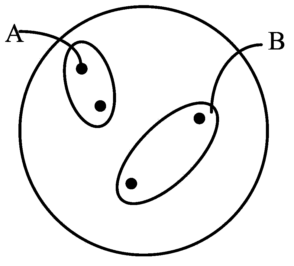
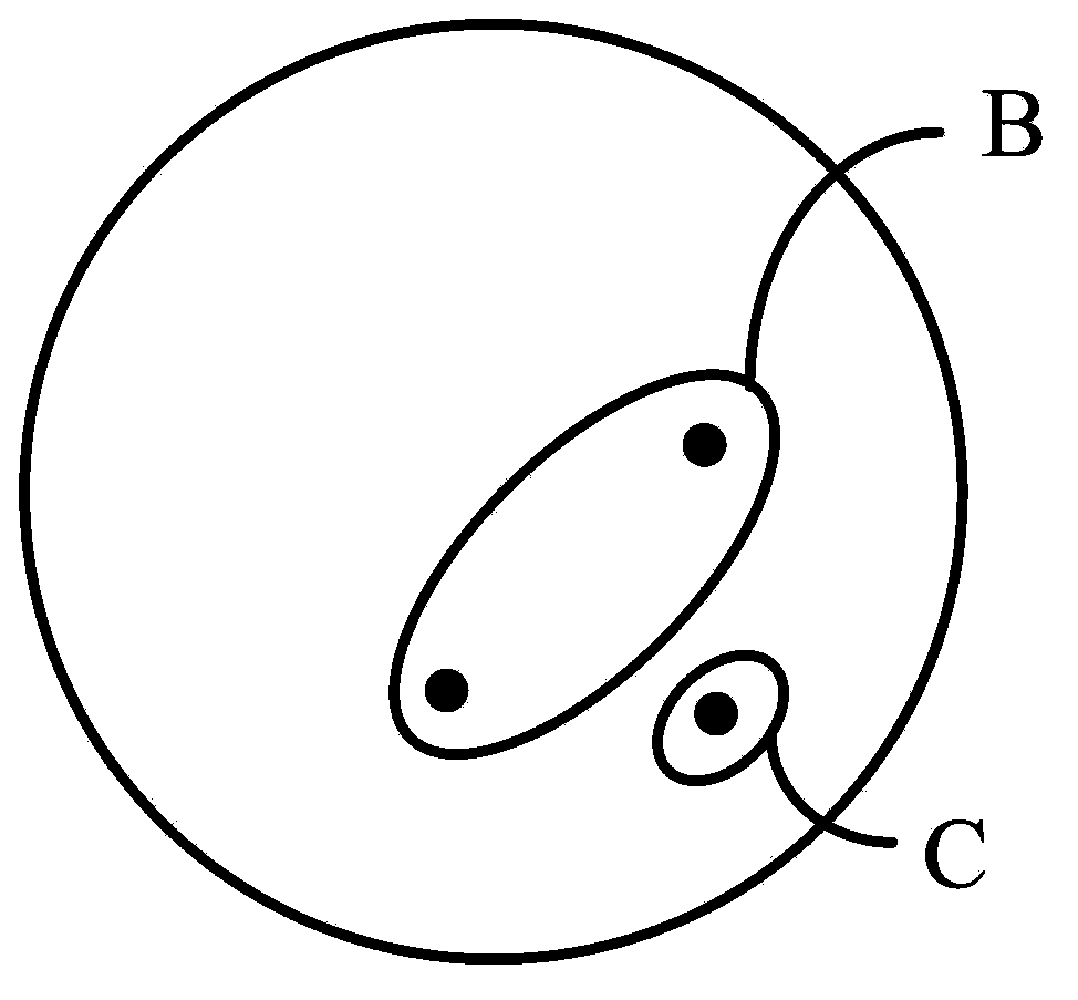
[0038] S3. Perform overlay calculation on the pre-value map and the post-value map to obtain the overlay and corresponding overlay values, wherein the overlay value is the number of newly added defects in the two processes;

[0039] S4. Comparing the overlay value with the system preset threshold spec, if the overlay value is less than or equal to spec, it is determined that the machine is normal; if the overlay value is g...


PUM


Abstract

The invention discloses a semiconductor equipment machine quality monitoring method and system. The method comprises: S1, automatically obtaining previous value data of machine quality monitoring in a previous process and back value data of machine quality monitoring in a later process; S2, accordingly generating a previous value graph and a back value graph from the previous value data and the back value data; S3, performing overlay calculation on the previous value graph and the back value graph, and obtaining an overlay graph and a corresponding overlay graph value; and S4, comparing the overlay graph value and a threshold spec set by a system in advance, if the overlay graph value is smaller than or equal to the spec, determining that a machine is normal, and if the overlay graph value is greater than the spec, determining that the machine is abnormal, and the machine stopping operation. By using the method and system provided by the invention, data can be collected in real time and automatically monitored, the collected data is accurate and complete, errors caused by manual recording are eliminated, and at the same time, when generated defects exceed a system preset value, the operation of the machine is stopped so that the product yield rate of wafer production is improved.

Description

technical field [0001] The invention relates to the technical field of semiconductor equipment, in particular to a method and system for monitoring the quality of a semiconductor equipment machine. Background technique [0002] Some crystal defects are caused by changes in temperature, pressure, medium component concentration, process equipment, operators, factory environment, etc. during the wafer process; some are caused by the thermal movement or produced by stress. They can migrate in the crystal lattice, so that they disappear, and new defects can be generated at the same time. [0003] The existence of crystal defects will have a significant impact on the properties of crystals. Actual crystals have more or less defects. The existence of some point defects in an appropriate amount can greatly enhance the conductivity of semiconductor materials and the luminescence of luminescent materials, and play a beneficial role; while the existence of defects such as dislocatio...

Claims


Application Information

Patent Timeline
Patent Type & Authority Applications(China)
IPC IPC(8): G05B19/406
Inventor 栾广庆
Owner CSMC TECH FAB2 CO LTD
Why Eureka
Try Eureka