
Nanolithography alignment method based on tiled-grating moire fringe phase demodulation

A moiré fringe and phase demodulation technology, which is applied in the photoplate making process, optics, instruments and other directions of the pattern surface, can solve the problems that affect the alignment accuracy and reduce the alignment efficiency, so as to improve the accuracy and efficiency and avoid scanning , the effect of high sensitivity

Inactive Publication Date: 2014-06-04
INST OF OPTICS & ELECTRONICS - CHINESE ACAD OF SCI
View PDF5 Cites 0 Cited by
  • Summary
  • Abstract
  • Description
  • Claims
  • Application Information

AI Technical Summary

Problems solved by technology

[0003] The current optical projection lithography machines generally use the scanning method of the workpiece table to achieve alignment, which reduces the alignment efficiency, and the drift error of the workpiece table introduced during the scanning process will affect the alignment accuracy

Method used


Image

  • Nanolithography alignment method based on tiled-grating moire fringe phase demodulation
  • Nanolithography alignment method based on tiled-grating moire fringe phase demodulation
  • Nanolithography alignment method based on tiled-grating moire fringe phase demodulation

Examples


Embodiment Construction

[0014] In order to make the object, technical solution and advantages of the present invention clearer, the present invention will be further described in detail below in conjunction with specific embodiments and with reference to the accompanying drawings.

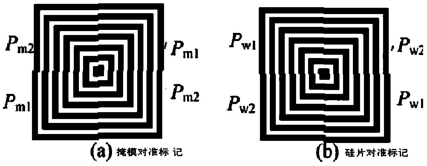
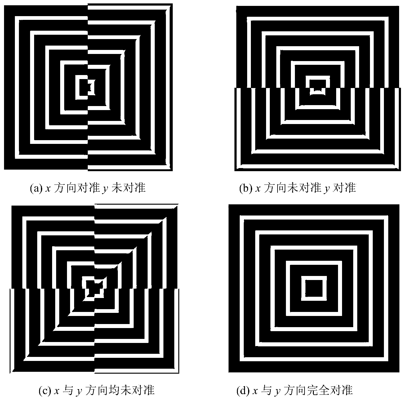
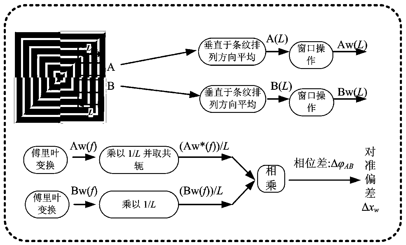
[0015] like Figure 4 Alignment deviation Δx of mask-substrate center in x and y directions shown w , Δy w , the azimuth angle of the substrate relative to the mask is α. The two fixed points on the substrate are A(x A ,y A ), B(x B ,y B ), when there is no misalignment between the mask and the substrate, the point on the mask corresponding to the fixed points A and B on the substrate is A’(x’ A ,y' A ), B'(x' B ,y' B ). Make alignment marks at A, B, A', B' respectively. marked according to figure 1 The structure shown is fabricated. Among them, due to the deviation x and y directions are not aligned, the marks of A and A' will be produced as figure 2 (c) Moiré fringes shown. The same is true for B and B'....


PUM


Abstract

The invention discloses a nanolithography alignment method based on tiled-grating moire fringe phase demodulation. The method comprises the following steps: a tiled-grating is taken as a mask-workpiece stage alignment mark, moire fringe phase information is taken as a mask-workpiece stage alignment error carrier, the alignment error is directly calculated between a mask and a substrate through multi-pixel point phase extraction, so that the rapid alignment of the mask-worktable is realized. According to the method, dependence on precision and speed indexes of a workpiece stage is reduced, the alignment accuracy is guaranteed, and the alignment efficiency is improved.

Description

technical field [0001] The invention is applicable to the alignment of projection lithography optical systems, and belongs to the field of ultra-large-scale integrated circuit manufacturing and nano-device manufacturing in optical micro-processing technology. Background technique [0002] Lithography technology is the core technology of microelectronics manufacturing and information industry. As the mainstream lithography technology for large-scale integrated circuit production, since the birth of optical projection lithography technology in 1978, it has evolved from the original g-line and i-line lithography machines to Developed to the current ArF immersion lithography machine. Optical projection lithography has become the most widely used and fastest technologically advanced optical lithography technology today, and its resolution has also been extended from the initial tens of microns to the current 32nm, 22nm or even higher. The three major indicators to measure the pe...

Claims


Application Information

Patent Timeline
Patent Type & Authority Applications(China)
IPC IPC(8): G03F9/00
Inventor 程依光朱江平胡松赵立新陈磊刘俊伯
Owner INST OF OPTICS & ELECTRONICS - CHINESE ACAD OF SCI
Learn More