Method and device for electroplating blind holes

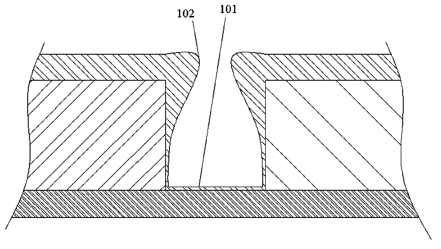
A technology of blind holes and electroplating units, which is applied in the direction of electrical connection formation of printed components, can solve problems such as insufficient copper thickness of copper layer 101, sealing of blind holes, thick deposition of copper layer 102, etc., so as to avoid sealing phenomenon and improve yield rate Effect

Active Publication Date: 2014-06-04
SHENNAN CIRCUITS
View PDF3 Cites 6 Cited by
  • Summary
  • Abstract
  • Description
  • Claims
  • Application Information

AI Technical Summary

Problems solved by technology

However, if figure 1 As shown, because the electroplating process is affected by the distribution of the circuit pattern and the current distribution, sometimes the copper thickness of the copper layer 101 at the bottom of the blind hole ...

Method used


Image

  • Method and device for electroplating blind holes
  • Method and device for electroplating blind holes
  • Method and device for electroplating blind holes

Examples


Embodiment Construction

[0030] Embodiments are listed below, and the present invention is described in detail in conjunction with the accompanying drawings.

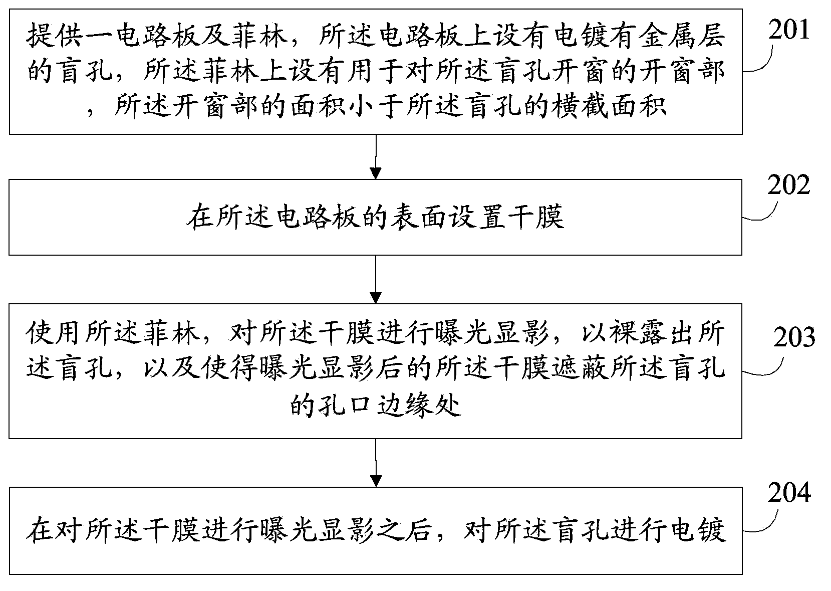
[0031] Such as figure 2 As shown, a method for electroplating blind holes includes:

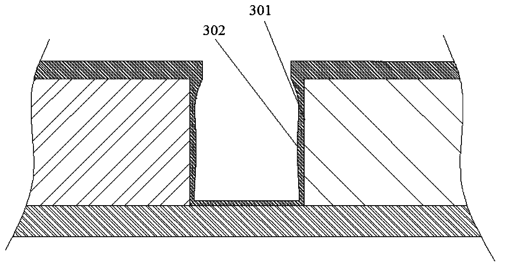
[0032] 201. If Figure 3a As shown, provide a circuit board and film ( Figure 3a not shown), the circuit board is provided with a blind hole 302 electroplated with a metal layer 301, and the film is provided with a window opening for opening a window to the blind hole, and the area of ​​the window opening is smaller than the The cross-sectional area of ​​the blind hole.

[0033] Before implementing this embodiment, the blind hole is thickened and electroplated twice as needed, and a pattern for opening a window to the blind hole is formed on the film, that is, a window opening part for opening a window to the blind hole is formed. Wherein, the area of ​​the window portion on the film used to open a window for the blind hole is smaller than the cross-sect...


PUM


Abstract

The invention discloses a method for electroplating blind holes. The method comprises: providing a circuit board equipped equipped with blind holes with an electroplated metal layer; providing a film provided with an open window opened to the blind holes, wherein the area of the open window is smaller than the cross-sectional area of the blind holes; providing a dry film on the surface of the circuit board; using the film to perform exposure and development on the dry film, enabling the orifice edge of the blind hole to be shielded by the dry film that has been exposed and developed; and electroplating the blind holes after the dry film is exposed and developed. The invention further provides a device for electroplating the blind holes. According to the invention, the bottom copper layer of the blind holes is thickened, the orifice edge of the blind holes is prevented from being thickened, the sealing phenomenon is avoided, and the yield of the circuit board is improved.

Description

technical field [0001] The invention relates to a method and a device for making a circuit board, in particular to a method and a device for electroplating blind holes. Background technique [0002] At present, in the process of manufacturing circuit boards with blind holes, VCP plating (Vertical Continuous Plating, vertical continuous plating) blind holes is generally used first, and then circuit pattern plating is performed to obtain the circuit board to be prepared. However, if figure 1 As shown, because the electroplating process is affected by the distribution of the circuit pattern and the current distribution, sometimes the copper thickness of the copper layer 101 at the bottom of the blind hole is not enough after electroplating, and the copper layer 102 at the edge of the blind hole is deposited too thickly, and even blind holes appear. Pore ​​sealing phenomenon, which will make subsequent processes such as surface coating impossible. Contents of the invention ...

Claims


Application Information

Patent Timeline
IPC IPC(8): H05K3/42
Inventor 黄蕾沙雷
Owner SHENNAN CIRCUITS
Why Eureka
Try Eureka