
Acceleration sensor

An acceleration sensor and area technology, which is applied in the measurement of acceleration, multi-dimensional acceleration measurement, speed/acceleration/impact measurement, etc., can solve the problem of inability to obtain a large air damping effect, and achieve the effect of reducing air damping

Active Publication Date: 2014-06-04
FUJI ELECTRIC CO LTD
View PDF6 Cites 1 Cited by
  • Summary
  • Abstract
  • Description
  • Claims
  • Application Information

AI Technical Summary

Problems solved by technology

[0008] However, in the conventional example described in the above-mentioned Patent Document 1, although air damping can be reduced by utilizing the through holes formed in the movable electrode and the fixed electrode, there is an unsolved problem as follows: Since only one Through holes, so the effect of reducing air damping is small, and when the movable electrode vibrates at a high frequency, a large air damping effect cannot be obtained

Method used


Image

  • Acceleration sensor
  • Acceleration sensor
  • Acceleration sensor

Examples


Embodiment Construction

[0025] Embodiments of the present invention will be described below based on the drawings.

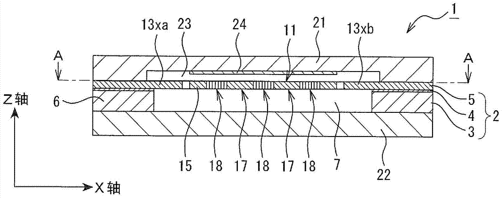
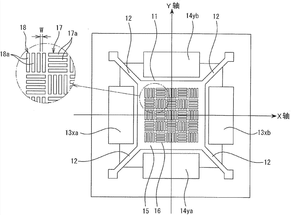
[0026] figure 1 is a sectional view showing an example of an acceleration sensor according to the present invention, figure 2 yes figure 1 End view of the A-A line.

[0027] In the figure, 1 is an acceleration sensor, and the acceleration sensor 1 is formed on an SOI (Silicon On Insulator: silicon on insulator) substrate 2 . The SOI substrate 2 is composed of an underlying silicon support layer 3 , a silicon oxide layer 4 formed on the silicon support layer 3 , and an active silicon layer 5 formed on the silicon oxide layer 4 .

[0028] In addition, the square frame-shaped portion 6 on the outer peripheral side of the silicon supporting layer 3 and the silicon oxide layer 4 is left, and the central portion is removed by etching to form a space portion 7 .

[0029] On the other hand, for the active silicon layer 5 on the upper part, for example, use anisotropic dry etching to remov...


PUM


Abstract

An acceleration sensor, which enables rigidity to be ensured while forming multiple through-holes on a movable electrode, is provided. A silicon oxide layer (4) is formed on a silicon support layer (3). A Silicon on Insulator (SOI) substrate (2) having an active silicon layer (5) formed on the silicon oxide layer is provided. A movable electrode (11) constituted by a weight supported by elastic beams, and fixed electrodes (13xa, 13xb, 14ya, 14yb), which are fixed in a position facing the periphery of the movable electrode, are formed on the active silicon layer of the SOI substrate. Through-holes (16) that penetrate in the Z-axis direction are formed over the entire surface on the inside of an outer peripheral part where the elastic beams (12) of the movable electrode are linked.

Description

technical field [0001] The present invention relates to an acceleration sensor. The acceleration sensor comprises an SOI substrate formed by forming a silicon oxide layer on a silicon support layer, and forming an active silicon layer on the silicon oxide layer, and forming an active silicon layer on the SOI substrate. There are movable electrodes and fixed electrodes opposite to its periphery. Background technique [0002] As such an acceleration sensor, a capacitive semiconductor sensor has been proposed in which a fixed electrode and a movable electrode spaced from the inside and outside of the fixed electrode by a predetermined distance are arranged so that their detection surfaces face each other. , and form a through hole penetrating from the detection surface of the movable electrode and the fixed electrode to the surface opposite to the detection surface, thereby reducing the air damping generated between the movable electrode and the fixed electrode (for example, re...

Claims


Application Information

Patent Timeline
Patent Type & Authority Applications(China)
IPC IPC(8): G01P15/125G01P15/18H01L29/84
CPCG01P2015/084G01P2015/0871G01P15/18G01P15/125G01P2015/0882
Inventor 坂上智矢尾博信木代雅巳铃木健
Owner FUJI ELECTRIC CO LTD
Learn More