Peripheral circuit structure

A peripheral circuit and peripheral technology, applied in the direction of printed circuit components, static electricity, electrical components, etc., can solve problems such as damage, electrostatic discharge damage of peripheral circuit structures, etc., to increase circulation paths, improve anti-static discharge capabilities, and improve reliability Effect

Active Publication Date: 2014-06-18
WINTEK CHINA TECH LTD +1
View PDF4 Cites 4 Cited by
  • Summary
  • Abstract
  • Description
  • Claims
  • Application Information

AI Technical Summary

Problems solved by technology

However, due to the difference in resistance between the trace and the pad, once the instantaneous current excessively accumulates at the joint between the two, the peripheral circuit struc

Method used


Image

  • Peripheral circuit structure
  • Peripheral circuit structure
  • Peripheral circuit structure

Examples


Embodiment Construction

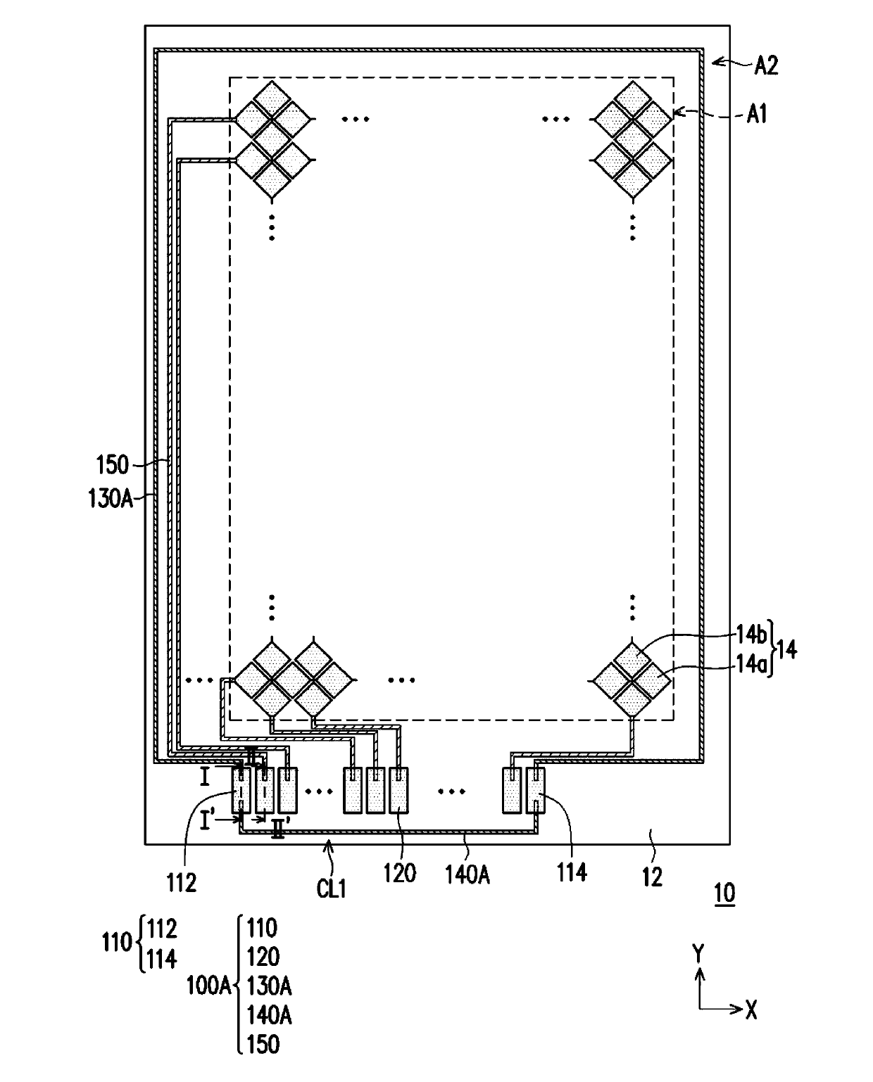
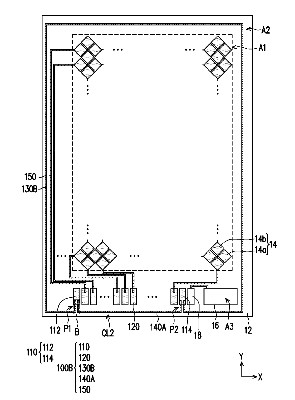
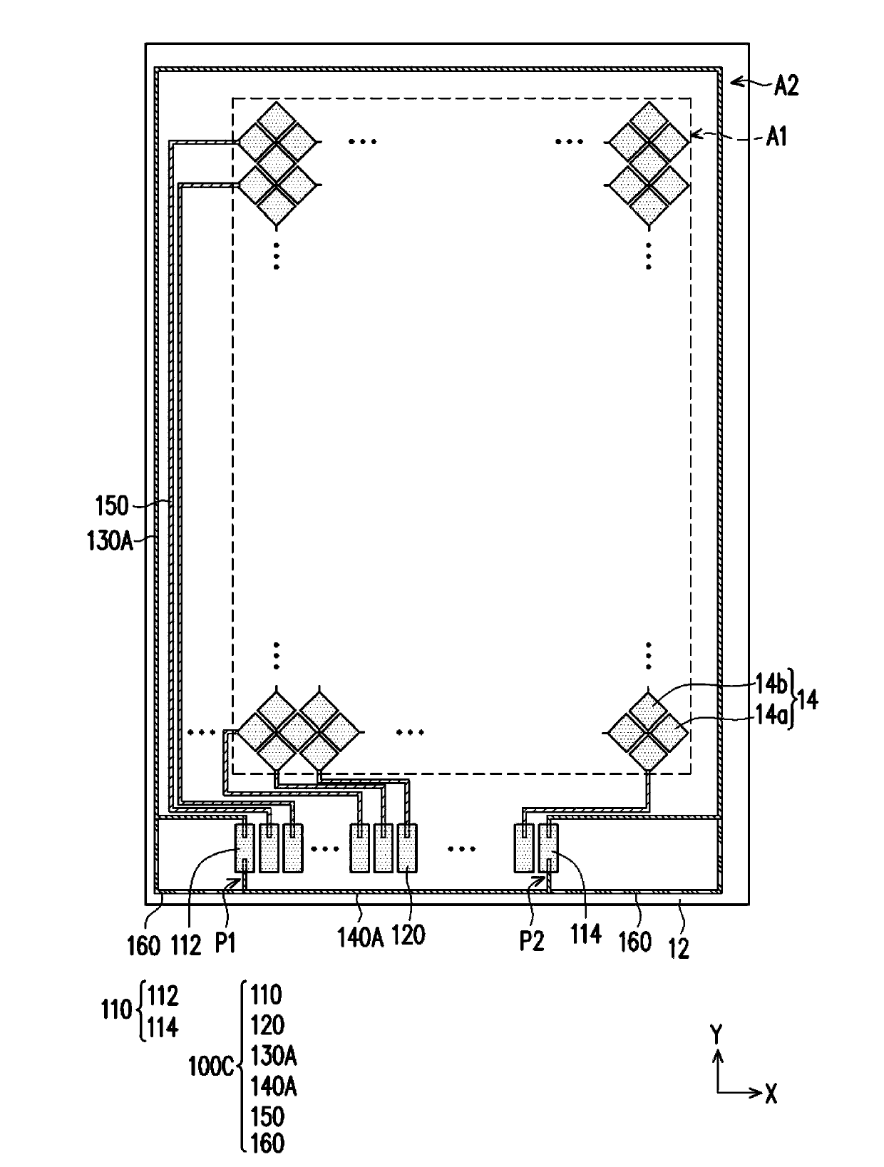
[0064] figure 1 It is a schematic top view of a touch panel applying the peripheral circuit structure of the embodiment of the present invention; figure 2 It is a schematic top view of a touch panel applying the peripheral circuit structure of the embodiment of the present invention; image 3 It is a schematic top view of a touch panel applying the peripheral circuit structure of the embodiment of the present invention; Figure 4A to Figure 4B It is a schematic top view of different touch panels applying the peripheral circuit structure of the embodiment of the present invention; Figure 5 It is a schematic top view of a touch panel applying the peripheral circuit structure of the embodiment of the present invention; Figure 6 It is a schematic top view of a touch panel applying the peripheral circuit structure of the embodiment of the present invention. Please refer to figure 1 For example, the peripheral circuit structure 100A of this embodiment can be applied in a touc...


PUM


Abstract

The invention provides a peripheral circuit structure which is arranged on a substrate. The substrate comprises a component region and a peripheral circuit region. The peripheral circuit structure in the peripheral circuit region comprises multiple first connecting pads, multiple second connecting pads, a first line, a second line and multiple third lines, wherein the multiple third lines are connected to components in the component region, and electrically connected with the second connecting pads. Each first connecting pad comprises a first grounding connection pad and a second grounding connection pad, and the second connecting pads are positioned between the first grounding connection pads and the second grounding connection pads. The two ends of the first line are respectively electrically connected with the first grounding connection pads and the second grounding connection pads. The two ends of the second line are also respectively electrically connected with the first grounding connection pads and the second grounding connection pads Thus, the second line, the first line, the first grounding connection pads and the second grounding connection pads form an enclosed loop.

Description

technical field [0001] The present invention relates to a peripheral circuit structure, and in particular to a peripheral circuit structure which helps to improve the ability of anti-electrostatic discharge (ESD). Background technique [0002] Generally speaking, electronic products may be damaged by electrostatic discharge at any time during production, packaging, testing, handling, and final assembly and use, resulting in the possibility of malfunctioning. Therefore, electronic products must have electrostatic discharge protection design in order to effectively prolong their service life. [0003] During the manufacturing process, an electrostatic discharge protection circuit is usually built around the electronic components to guide the current generated by the electrostatic discharge to the ground terminal and prevent the peripheral circuit structure from being damaged due to the current entering the internal circuit. [0004] ESD protection circuits usually consist of ...

Claims


Application Information

Patent Timeline
IPC IPC(8): H05K1/02H05F3/02
Inventor 李忠宪陈国兴陈昱廷苏振豪
Owner WINTEK CHINA TECH LTD
Why Eureka
Try Eureka