Nickel gold processing method for printed circuit board

A technology for printed circuit boards and processing methods, which is applied to the secondary processing of printed circuits, the reinforcement of conductive patterns, and the application of non-metallic protective layers, etc. problems, to achieve the effect of improving the excellent rate, eliminating voids, and improving the degree of bonding

Inactive Publication Date: 2014-06-25
SHENNAN CIRCUITS
View PDF6 Cites 7 Cited by
  • Summary
  • Abstract
  • Description
  • Claims
  • Application Information

AI Technical Summary

Problems solved by technology

However, in the production practice, it was found that during the transfer process of the solder resist pattern, the film attached to

Method used


Image

  • Nickel gold processing method for printed circuit board
  • Nickel gold processing method for printed circuit board
  • Nickel gold processing method for printed circuit board

Examples


Embodiment Construction

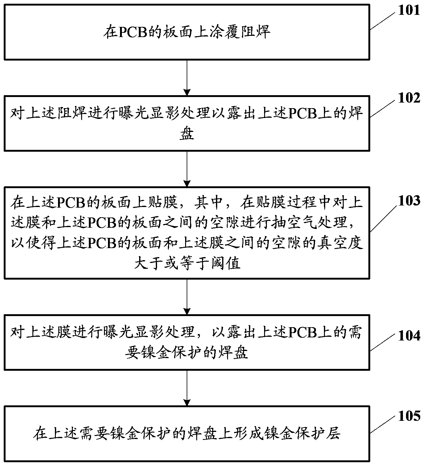
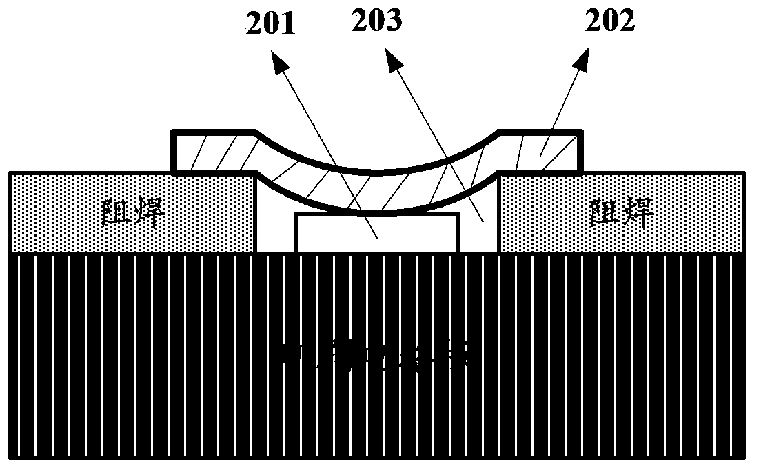
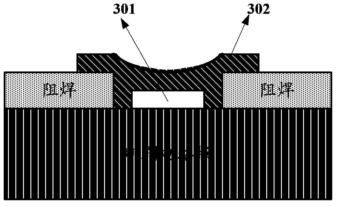
[0026] The embodiment of the present invention provides a nickel-gold treatment method for a printed circuit board, which is beneficial to reducing the cracking of the pad protection film and improving the product yield.

[0027] The following will clearly and completely describe the technical solutions in the embodiments of the present invention with reference to the accompanying drawings in the embodiments of the present invention. Obviously, the described embodiments are only some, not all, embodiments of the present invention. Based on the embodiments of the present invention, all other embodiments obtained by persons of ordinary skill in the art without creative efforts fall within the protection scope of the present invention.

[0028] The terms "first", "second", "third", "fourth", etc. (if any) in the description and claims of the present invention and the above drawings are used to distinguish similar objects and not necessarily Describe a specific order or sequence. ...


PUM


Abstract

The invention discloses a nickel gold processing method for a printed circuit board. The nickel gold processing method for the printed circuit board comprises steps that: a board surface of the printed circuit board is coated with resistance welding; exposure development treatment on the resistance welding is carried out to expose a welding disc on the printed circuit board; a film is pasted on the board surface of the printed circuit board, air extraction treatment on a gap between the film and the board surface of the printed circuit board is carried out in a film pasting process, so a vacuum degree of the gap between the film and the board surface of the printed circuit board is made to be greater than or equal to the threshold; exposure development treatment on the film is carried out to expose the welding disc needing nickel gold protection on the printed circuit board; a nickel gold protection layer is formed on the welding disc needing nickel gold protection. The nickel gold processing method facilitates to reduce break of a welding disc protection film and improves a product good rate.

Description

technical field [0001] The invention relates to the technical field of printed circuit board processing and manufacturing, in particular to a nickel-gold treatment method for printed circuit boards. Background technique [0002] When processing some electronic products, sometimes it is necessary to protect the large soldering pad with a dry film so that it will not be coated with nickel gold. When this type of product is processed in the solder mask process, the solder mask pattern will be transferred by opening a window . However, in the production practice, it was found that during the transfer process of the solder resist pattern, the film attached to the protective soldering pad was often broken, which eventually resulted in nickel-gold plating on the soldering copper pad, affecting product quality. Contents of the invention [0003] The embodiment of the present invention provides a nickel-gold treatment method for a printed circuit board, in order to reduce the crac...

Claims


Application Information

Patent Timeline
IPC IPC(8): H05K3/24H05K3/28
Inventor 高超柱饶猛沙雷
Owner SHENNAN CIRCUITS
Why Eureka
Try Eureka