Wafer-level CSP structure with insulated side wall and packaging method thereof
A technology of packaging structure and sidewall insulation, applied in electrical components, electrical solid devices, circuits, etc., can solve the problems of uneven heating temperature during reflow, unbalanced electrodes at both ends, chip leakage, etc., to eliminate the phenomenon of tin creep, overcome Leakage problem, the effect of reducing production cost
- Summary
- Abstract
- Description
- Claims
- Application Information
AI Technical Summary
Problems solved by technology
Method used
Image
Examples
Embodiment 1
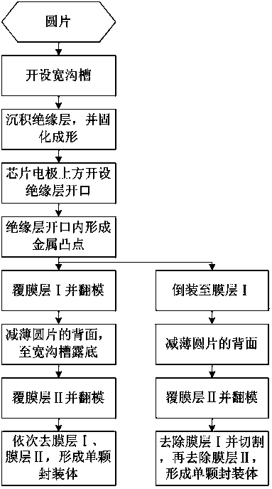
[0044] see figure 2 , a wafer-level CSP packaging method with sidewall insulation of the present invention, its technological process is as follows:
[0045] Executing step 1: providing a wafer with a chip electrode array;
[0046] Execute step 2: open a wide groove that does not cut through the wafer along the scribing lane of the wafer on the surface of the wafer;
[0047] Execute step 3: deposit an insulating layer on the surface of the wafer and the inner wall of the wide groove, and solidify and shape;
[0048] Executing step 4: opening an insulating layer opening through the insulating layer above the chip electrode;
[0049] Executing Step 5: Electroless plating of metal bumps in the opening of the insulating layer;
[0050] Execute Step 6: Cover the metal bumps with film layer I and turn over the mold so that the back of the wafer faces upwards;
[0051] Execute step 7: Thinning the back of the wafer until the bottom of the wide groove is exposed;
[0052] Execut...
Embodiment 2
[0068] see figure 2 , a wafer-level CSP packaging method with sidewall insulation of the present invention, its technological process is as follows:
[0069] Executing step 1: providing a wafer with a chip electrode array;
[0070] Execute step 2: open a wide groove that does not cut through the wafer along the scribing lane of the wafer on the surface of the wafer;
[0071] Execute step 3: deposit an insulating layer on the surface of the wafer and the inner wall of the wide groove, and solidify and shape;
[0072] Executing step 4: opening an insulating layer opening through the insulating layer above the chip electrode;
[0073] Executing Step 5: Electroless plating of metal bumps in the opening of the insulating layer;
[0074] Execute Step 6: Flip-chip to film layer Ⅰ, so that the back of the wafer faces up;
[0075] Execute step 7: Thinning the back side of the wafer;
[0076] Executing step 8: coating layer II on the back of the above-mentioned wafer and turning ...
Embodiment 3
[0086] Embodiment three, see Figure 28 and Figure 29
[0087] The difference between this embodiment and Embodiment 1 and Embodiment 2 is that: the surface of the silicon substrate 101 on the other side of the chip electrode 110 is provided with a back protection layer 130 to enhance the strength of the wafer-level CSP packaging structure.
[0088] The back protection layer is formed on the other side of the wafer 100 by film sticking or printing before coating the film layer II 520 on the surface of the wafer 100 , and is divided by a dicing knife or laser when forming the dividing lines.
PUM
| Property | Measurement | Unit |
|---|---|---|
| Depth | aaaaa | aaaaa |
Abstract
Description
Claims
Application Information


