Low-cost wafer-level CSP method and structure
A packaging structure and packaging method technology, applied in electrical components, electrical solid devices, circuits, etc., can solve problems such as imbalance at both ends of the electrode, uneven reflow heating temperature, chip leakage, etc., to reduce production costs and eliminate tin creep. phenomenon, the effect of improving the placement yield
- Summary
- Abstract
- Description
- Claims
- Application Information
AI Technical Summary
Problems solved by technology
Method used
Image
Examples
Embodiment 1
[0061] Adopt above-mentioned processing method, form embodiment one of the present invention, as follows:
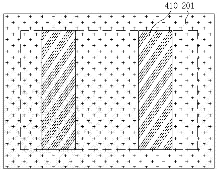
[0062] Such as image 3 and Figure 4 A low-cost wafer-level CSP packaging structure is shown, the silicon base body 101 has two chip electrodes 110, the surface of the chip electrodes 110 is provided with flat metal bumps 310, and the flat metal bumps 310 are made of metals such as nickel / gold Formed by electroless plating and mechanically ground, and fixed to the surface of the chip electrode 110 . The height h1 of the flat metal bump 310 is preferably 15 μm≤h1≤25 μm. The upper surface of the flat metal bump 310 is covered with metal such as copper as the metal protection layer 410 .
[0063] The sidewall of the silicon base body 101 on one side of the chip electrode 110 is stepped, and the step 121 is a first step, such as image 3 As shown, the chip electrode 110 is located on the top of the stepped silicon base body 101 . The step is part of a wide trench 120 f...
Embodiment 2
[0072] Embodiment two, see Figure 14
[0073] The low-cost wafer-level CSP packaging structure of the second embodiment is basically the same as that of the first embodiment. The difference between the two is that the surface of the silicon base body 101 located on the other side of the chip electrode 110 is provided with a back protective layer 421 to enhance the roundness. The strength of the chip-level CSP package structure.
[0074] The back protection layer is formed on the other side of the wafer 100 by film sticking or printing before the chemically plated metal bumps 300 on the surface of the wafer 100 , and is divided by a dicing knife or laser when forming the dividing lines 521 .
Embodiment 3
[0075] Embodiment three, see Figure 15
[0076] The difference between this embodiment and Embodiment 1 and Embodiment 2 is that each chip 11 can also be designed with three or more chip electrodes, and the chip electrodes 110 are distributed in an array on the silicon base body 101 . Such as Figure 15 As shown, each chip 11 is designed with six chip electrodes 110 to meet the needs of product applications.
[0077] A low-cost wafer-level CSP packaging method of the present invention and its packaging structure are not limited to the above-mentioned preferred embodiments. For example, the step 121 can be more than one step. When the step is more than ten steps, the silicon formed by the wafer-level process is basically The side wall of the body 101 is slope-shaped, such as Figure 16 As shown, the more steps there are on the sidewall of the silicon base body 101, the more favorable the combination of the insulating material and the silicon base body 101 is. The total dept...
PUM
 Abstract
Description
Claims
Application Information


