An interface circuit capable of tolerating high voltage input

An interface circuit and high-voltage technology, applied in the field of interface circuits, can solve problems such as occupying chip area and complicated circuit control, and achieve the effects of solving leakage problems, speeding up transformation, and improving anti-noise and anti-latch-up capabilities

Inactive Publication Date: 2009-10-07
BEIJING MXTRONICS CORP +1
View PDF0 Cites 24 Cited by
  • Summary
  • Abstract
  • Description
  • Claims
  • Application Information

AI Technical Summary

Problems solved by technology

Existing NMOS-blocking technology, such as the dynamic gate bias mentioned in "A new charge pump circuit dealing with gate-oxide reliability issue in low-voltage processes" published by M.-D.Ker on circuits and systems in 2004 Circuits and charge pump circuits, etc., although high withstand voltage design can be realized, a large number of auxiliary circuits are needed to achieve protection purposes, the circuit control is complicated, and it will occupy a large amount of chip area

Method used


Image

  • An interface circuit capable of tolerating high voltage input

Examples


Embodiment Construction

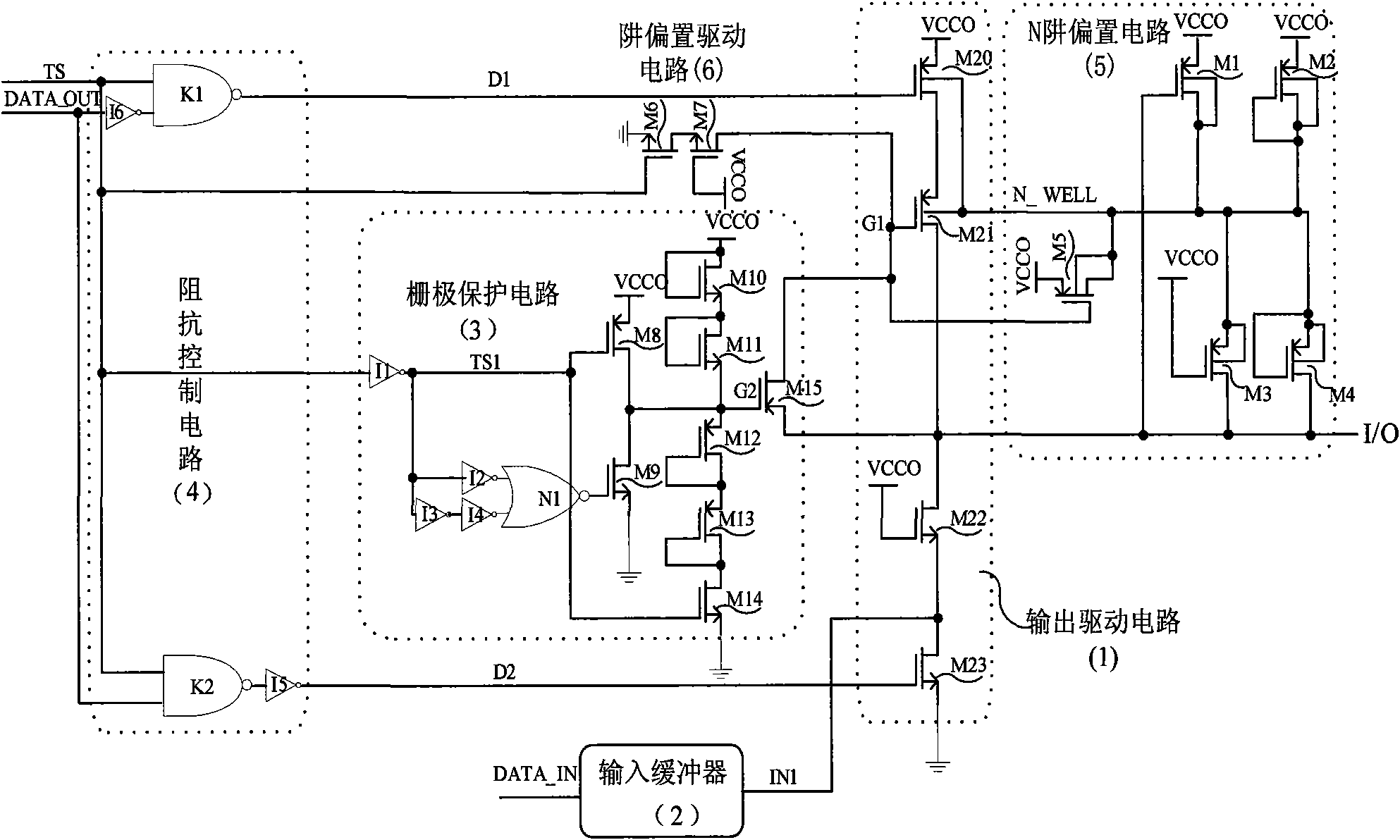
[0021] Such as figure 1 As shown, it is a functional block diagram of an interface circuit that can withstand high voltage input in the present invention, including an output drive circuit 1, an input buffer 2, a gate protection circuit 3, an impedance control circuit 4, an N well bias circuit 5 and a well bias circuit Set the drive circuit 6. Under the control of the mode control signal TS, the interface circuit can be in the transmission mode (that is, the I / O pin is used as an output pin), or in the reception mode (that is, the I / O pin is used as an input pin). When the circuit is in transfer mode, the DATA_OUT signal is the data output signal. When the circuit is in the receiving mode, the DATA_IN signal receives external signals and inputs them into the interface circuit.

[0022]If the mode control signal TS sets the interface circuit to the transmission mode, the impedance control circuit 4 receives the data output signal DATA_OUT generated by the configurable logic m...


PUM


Abstract

An interface circuit capable of tolerating high voltage input, I / O pin connecting external, a pull-up / pull-down structure provides high / low power level of output to the I / O pin. An impedance control circuit shuts the pull-up / pull-down structure in receiving mode, and activates the pull-up / pull-down structure in transmission mode. A pull-up / pull-down protection structure protects the pull-up / pull-down structure in receiving mode. A gate protection circuit provides protection voltage to the pull-up protection structure in receiving mode. A N-well bias circuit provides a bias voltage that equaling to internal power supply for the pull-up structure and the N-well where the PMOS located in of the pull-up protection structure in transmission mode; and in a receiving mode, if voltage of the I / O pin is higher than voltage of the internal power supply, providing a bias voltage that approaching to voltage of the I / O pin to the pull-up structure and the N-well where the PMOS located in of the pull-up protection structure, otherwise, providing a bias voltage that equaling to internal power supply. Well bias drive circuit provides driving signal to the N-well bias circuit in transmission mode.

Description

technical field [0001] The invention relates to an interface circuit capable of withstanding external high voltage input. Background technique [0002] With the continuous improvement of CMOS technology, the circuit design is rapidly evolving to deep submicron technology, and the power supply voltage is gradually reduced to 2.5V or 1.8V. However, some peripheral device chips still work at a higher voltage level, such as 3.3V or 5V, resulting in a system that may have different voltage standards running at the same time. For example, when a chip with an internal interface circuit operating voltage of 2.5V must be connected to a 3.3V or 5V external interface, or a chip with an internal interface circuit operating voltage of 3.3V must be connected to a 5V external interface, if If the withstand voltage problem is not considered in the chip I / O interface design, various problems will be caused, such as oxide layer breakdown, hot carrier degradation effect and leakage current, e...

Claims


Application Information

Patent Timeline
Patent Type & Authority Applications(China)
IPC IPC(8): H03K19/0185H03K3/02
Inventor 林彦君陈雷储鹏孙华波倪劼王雷
Owner BEIJING MXTRONICS CORP
Why Eureka
Try Eureka