Flexible circuit board and manufacturing method thereof

A technology of flexible circuit boards and manufacturing methods, which is applied in the direction of printed circuit manufacturing, printed circuits, printed circuit components, etc., can solve problems such as yield reduction, hole shape deformation, etc., to improve efficiency, prevent hole shape deformation, and excellent quality Effect

Inactive Publication Date: 2014-07-02
AVARY HLDG (SHENZHEN) CO LTD +1
View PDF6 Cites 10 Cited by
  • Summary
  • Abstract
  • Description
  • Claims
  • Application Information

AI Technical Summary

Problems solved by technology

Since the Teflon layer of the outer layer has a weak ability to absorb laser energy, while the polyimide layer of the inner layer has a stronger ability to absorb laser energy, so when performing laser etching, the polyimide layer of the inner layer Compared with the outer Teflon layer, the polyimide layer absorbs more energy, which causes the polyimide layer to shrink too much, which leads to the deformation of the hole shape and reduces the yield.

Method used


Image

  • Flexible circuit board and manufacturing method thereof
  • Flexible circuit board and manufacturing method thereof
  • Flexible circuit board and manufacturing method thereof

Examples


Embodiment Construction

[0016] see Figure 1 to Figure 6 , an embodiment of the present invention provides a method for manufacturing a flexible circuit board, comprising the following steps:

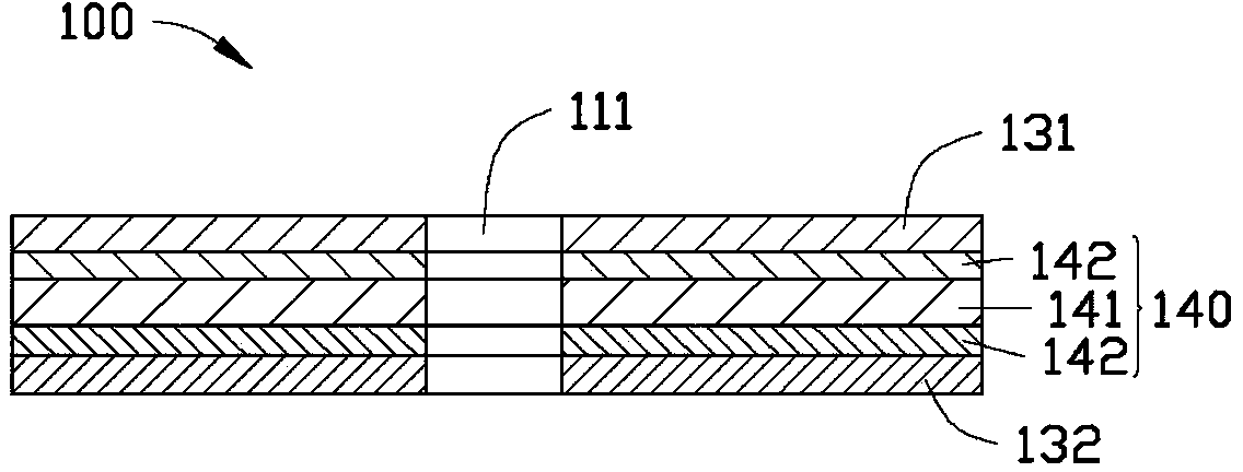
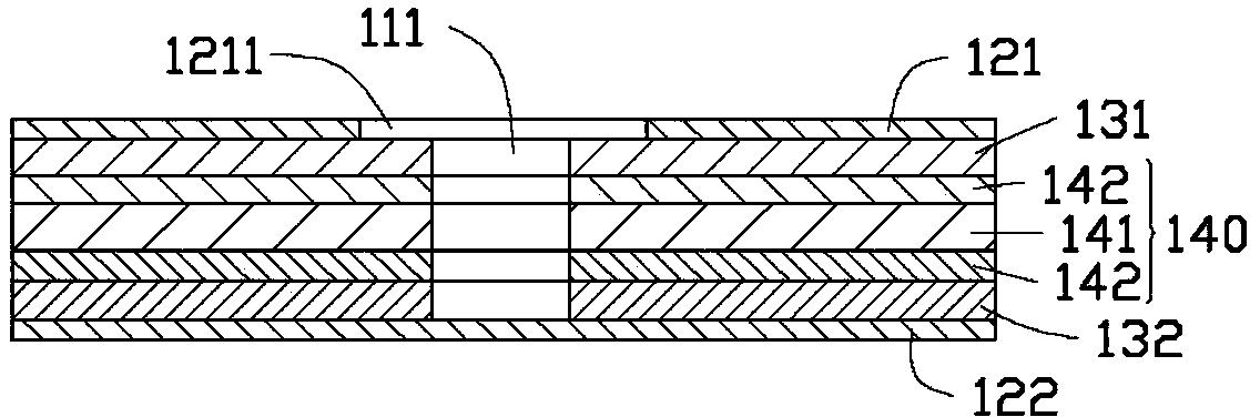
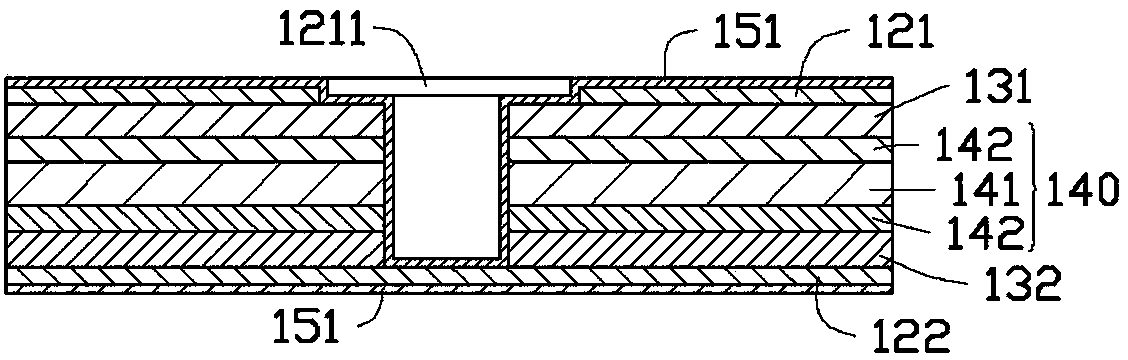
[0017] Step 1: See figure 1 , providing a flexible double-sided copper-clad substrate 100 , using a mechanical drilling method to make through holes 111 in the flexible double-sided copper-clad substrate 100 .

[0018] The flexible double-sided copper-clad substrate 100 includes an insulating base layer 140 and a first copper foil layer 131 and a second copper foil layer 132 disposed on opposite sides of the insulating base layer 140 . The insulating base layer 140 includes a polyimide layer 141 and a Teflon layer 142 arranged on opposite sides of the polyimide layer 141. In this embodiment, the Teflon layer 142 has a thickness of 6.25 microns, and The thickness of the imide layer 141 is 12.5 microns, and the ratio of the thickness of each Teflon layer to the polyimide layer is 1:2. The first copper foil la...


PUM


Abstract

A manufacturing method of a flexible circuit board comprises the following steps: providing a flexible double-faced copper-coated substrate, wherein the double-faced copper-coated substrate comprises an insulation base layer and a first copper foil layer and a second copper foil layer which are arranged at the opposite two sides of the insulation base layer, and the insulation base layer comprises a polyimide layer and Teflon layers which are arranged at the opposite two sides of the polyimide layer; manufacturing a through-hole by utilizing a mechanical drilling method; covering a first anti-coating layer and a second anti-coating layer on the surface of the first copper foil layer and the surface of the second copper foil layer respectively; forming a continuous conductive film on the inner wall of the through-hole and the surface of the second anti-coating layer in the through-hole; forming an electroplated metal layer on the conductive film by utilizing an electroplating method, the conductive film and the electroplated metal layer forming a conductive blind hole; removing the first anti-coating layer and the second anti-coating layer; and enabling the first copper foil layer and the second copper foil layer to be made into a first conductive circuit pattern and a second conductive circuit pattern respectively, and thus the flexible circuit board is obtained. The invention also relates to the flexible circuit board formed by utilizing the above method.

Description

technical field [0001] The invention relates to a method for manufacturing a circuit board, in particular to a flexible circuit board and a method for manufacturing the same. Background technique [0002] Teflon base (teflon base) insulating material is often used as the base layer material in the development of high-frequency flexible circuit boards. The base layer material includes a polyimide (Polyimide, PI) layer and two layers respectively arranged on the polyimide Teflon layers on opposite sides of the imide layer. In the manufacturing process of flexible circuit boards, laser etching technology is often used to form blind holes in the base layer, and then the inner wall of the blind holes is electroplated to form conductive blind holes. Since the Teflon layer of the outer layer has a weak ability to absorb laser energy, while the polyimide layer of the inner layer has a stronger ability to absorb laser energy, so when performing laser etching, the polyimide layer of ...

Claims


Application Information

Patent Timeline
Patent Type & Authority Applications(China)
IPC IPC(8): H05K3/00H05K3/42H05K1/02H05K1/11
Inventor 李明何明展
Owner AVARY HLDG (SHENZHEN) CO LTD
Why Eureka
Try Eureka