Flash memorizer

A technology of flash memory and the middle part, which is applied in the field of flash memory, can solve problems such as threshold voltage drift, affect the electrical characteristics of storage devices, and data interference, and achieve resistance to threshold voltage drift, suppression of short-channel effects, and reduction of readout errors Effect

Active Publication Date: 2014-07-09
SHANGHAI HUALI MICROELECTRONICS CORP
View PDF3 Cites 8 Cited by
  • Summary
  • Abstract
  • Description
  • Claims
  • Application Information

AI Technical Summary

Problems solved by technology

There are inherent defects in the flash memory technology of floating gate transistors. The thin dielectric layer below 100 nanometers will cause leakage, which will lead to data interference and chip failure results.
In addition, devices below the sub-100nm technology node will have a more serious short channel effect (Short Channel Effect), which affects the electrical characteristics of the storage device, making its threshold voltage drift compared with the long channel, resulting in possible readout errors

Method used


Image

  • Flash memorizer
  • Flash memorizer
  • Flash memorizer

Examples


Embodiment Construction

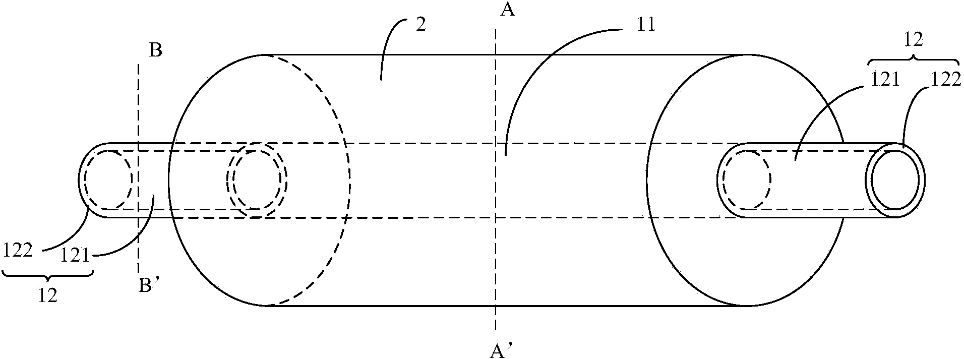
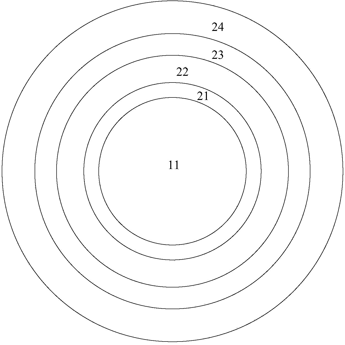
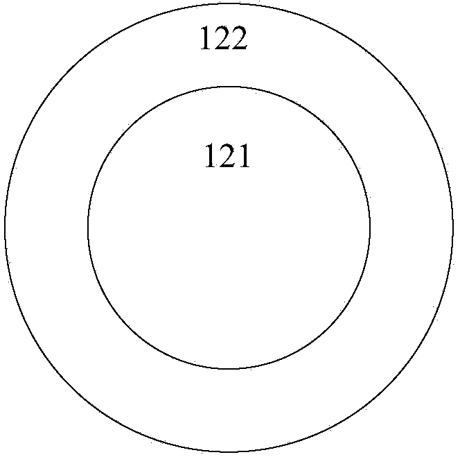
[0016] The flash memory of the present invention will be described in more detail below in conjunction with schematic diagrams, which represent preferred embodiments of the present invention. It should be understood that those skilled in the art can modify the present invention described here while still achieving the beneficial effects of the present invention. Therefore, the following description should be understood as the broad knowledge of those skilled in the art, but not as a limitation of the present invention.

[0017] In the interest of clarity, not all features of an actual implementation are described. In the following description, well-known functions and constructions are not described in detail since they would obscure the invention with unnecessary detail. It should be appreciated that in the development of any actual embodiment, numerous implementation details must be worked out to achieve the developer's specific goals, such as changing from one embodiment to...


PUM


Abstract

The invention discloses a flash memorizer. The flash memorizer comprises a cylindrical body structure serving as a substrate, wherein the body structure is of an N type silicon structure and comprises a middle portion and two end portions on the two sides of the middle portion, a grid electrode is wrapped on the middle portion in a surrounding mode to form a surrounding grid. The two end portions serve as a source electrode and a drain electrode and respectively comprise a layer of P type doped area. The portion, surrounded by the corresponding P type doped area, of each end portion is led out through a contact line and used for exerting a substrate voltage. A smaller grid length can be obtained, the voltages used for controlling the grid and a floating grid can well control a groove, the percentage of the portion, occupied by a source and drain depletion region through extension, of the total size of the depletion region can be lowered, the short-channel effect can be restrained, threshold voltage drift can be resisted, and reading mistakes of the flash can be reduced.

Description

technical field [0001] The invention relates to the technical field of semiconductors, in particular to a flash memory. Background technique [0002] For NOR flash memory cells, the most important limit to the continued reduction in size is the shortening of the gate length. This is mainly because the channel thermal electron (CHE) injection compilation method requires a certain voltage at the drain terminal, and this voltage has a great influence on the penetration of the source and drain terminals. For short channel devices, the channel thermal electron (CHE) method Not applicable. Another problem is that this limits the programming rate of NOR flash compared to NAND and AND data storage devices. According to the prediction of the document "G. Servalli, et al., IEDM Tech. Dig., 35_1, 2005", the physical limit of the gate length reduction of the traditional flash memory structure is 130nm. [0003] Existing flash memory storage units generally use polysilicon as a floati...

Claims


Application Information

Patent Timeline
Patent Type & Authority Applications(China)
IPC IPC(8): H01L27/115H01L29/423
Inventor 顾经纶
Owner SHANGHAI HUALI MICROELECTRONICS CORP
Why Eureka
Try Eureka