Physics-of-failure-based MOS (metal oxide semiconductor) device reliability simulation evaluation method

A technology of MOS devices and failure physics, applied in software simulation/interpretation/simulation, instrumentation, electrical digital data processing, etc., can solve the problems of only considering and not considering the failure of package interconnection, etc.

Inactive Publication Date: 2014-07-30
BEIHANG UNIV
View PDF2 Cites 34 Cited by
  • Summary
  • Abstract
  • Description
  • Claims
  • Application Information

AI Technical Summary

Problems solved by technology

However, the analysis shows that these algorithms mainly have the following two problems: 1. The analysis object of these methods is the chip, so only one or several failure mechanisms in the MOS structure of the chip are considered. Interconnection

Method used


Image

  • Physics-of-failure-based MOS (metal oxide semiconductor) device reliability simulation evaluation method
  • Physics-of-failure-based MOS (metal oxide semiconductor) device reliability simulation evaluation method
  • Physics-of-failure-based MOS (metal oxide semiconductor) device reliability simulation evaluation method

Examples


Embodiment Construction

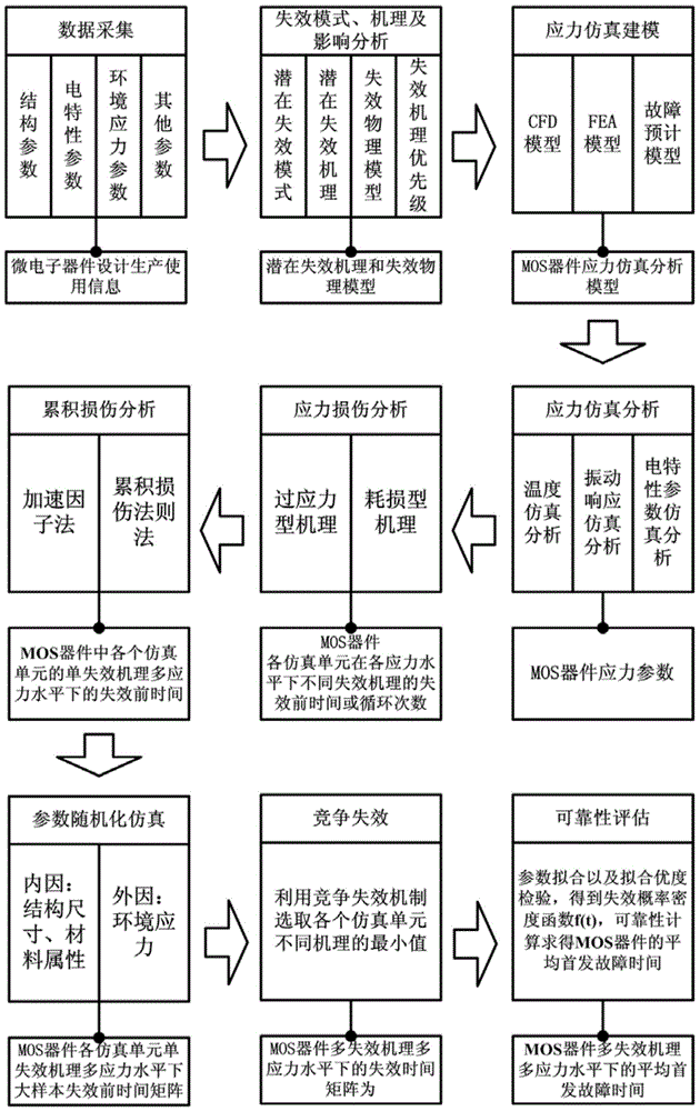
[0082] In the following, the present invention will be further described in detail in combination with the accompanying drawings and a reliability simulation evaluation case of a typical MOS device.

[0083] A kind of MOS device reliability simulation evaluation method based on failure physics of the present invention, concrete steps are as follows:

[0084] Step 1: Data Collection

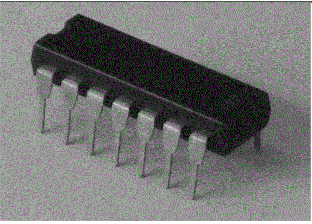
[0085] Such as figure 2 As shown, a certain type of device is selected as a case for reliability simulation evaluation. The device is a 42-input NOR gate and a 14-pin plastic-encapsulated dual in-line plug (DIP) device. The present invention will be described in detail below. Through device manuals, layout design documents, design experience and formula calculations, the relevant data collection results of MOS device reliability simulation evaluation are as follows:

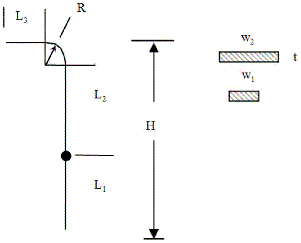
[0086] 1) Device structure parameters

[0087] MOS device structure information includes device package size and layout size in...


PUM


Abstract

The invention relates to a physics-of-failure-based MOS (metal oxide semiconductor) device reliability simulation evaluation method. The method comprises the following steps: first, acquiring related parameters of an MOS device; second, analyzing a failure mode, a mechanism and an influence; third, establishing CFD (computational fluid dynamics), FEA (finite element analysis) and failure prediction models; fourth, carrying out the simulation analysis on temperature, vibration and electrical characteristics; fifth, performing stress damage analysis; sixth, performing cumulative damage analysis; seventh, considering deviation and performing parameter randomization simulation; eighth, obtaining a time vector before a failure by utilizing a competition failure mechanism; ninth, estimating the average starting failure time of the device. According to the method, a potential failure mechanism and a corresponding failure physical model of the device are obtained by analyzing, the using stress of the device is determined by simulating and analyzing, and finally, the average starting failure time of the MOS device under using conditions is obtained by calculating from the possible failure reasons of the MOS device on the basis of a failure physical theory. The method belongs to the technical field of MOS device reliability simulation and evaluation.

Description

(1) Technical field: [0001] The invention relates to a failure physics-based MOS device reliability simulation evaluation method, which is based on the theory of failure physics, starting from the thermal, electrical and mechanical reasons that may cause failure in the actual use of MOS devices, and carries out failure modes, mechanisms and methods. The impact analysis obtains the potential failure mechanism of MOS devices and the corresponding failure physical model, obtains the use stress of the devices through simulation analysis, and finally obtains the average first failure time of MOS devices under actual use conditions through mathematical calculations. The method belongs to the technical field of MOS device reliability simulation evaluation. (2) Background technology: [0002] With the rapid development of microelectronic technology and integrated circuit industry, microelectronic devices have been used in all aspects of life due to their advantages such as simple pr...

Claims


Application Information

Patent Timeline
IPC IPC(8): G06F17/50G06F9/455G06F19/00
Inventor 付桂翠赵幼虎万博董一兵
Owner BEIHANG UNIV
Why Eureka
Try Eureka