Semiconductor element and manufacturing method thereof

A manufacturing method, semiconductor technology, applied in the direction of semiconductor devices, semiconductor/solid-state device manufacturing, electrical components, etc.

Active Publication Date: 2014-08-06
UNITED MICROELECTRONICS CORP
View PDF4 Cites 9 Cited by
  • Summary
  • Abstract
  • Description
  • Claims
  • Application Information

AI Technical Summary

Problems solved by technology

[0005] The purpose of the present invention is to provide a semiconductor structure and its manufacturing method to solve the problems encountered by semiconductor elements in the prior art

Method used


Image

  • Semiconductor element and manufacturing method thereof
  • Semiconductor element and manufacturing method thereof
  • Semiconductor element and manufacturing method thereof

Examples


Embodiment Construction

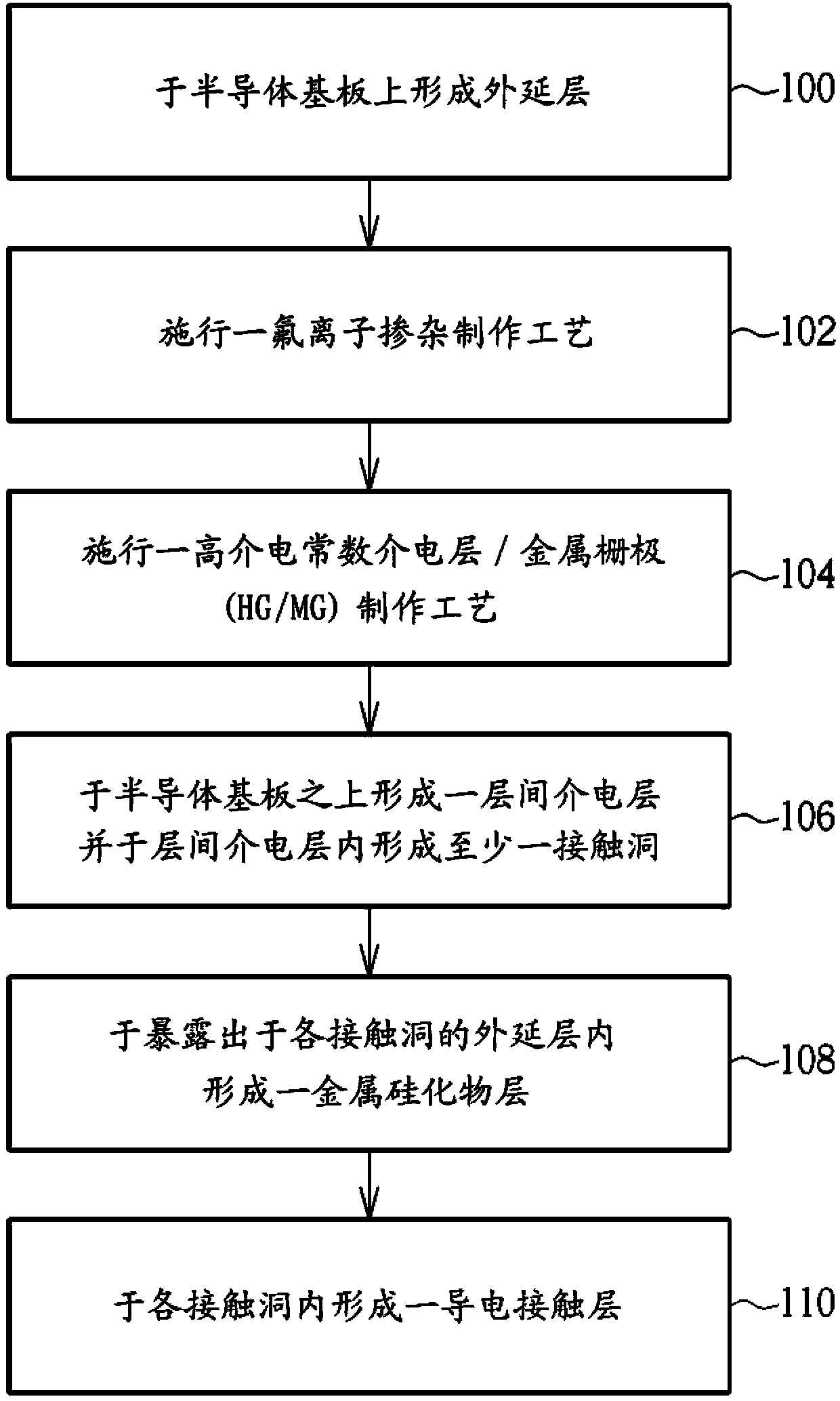
[0040] Hereinafter, specific implementations of the semiconductor device structure and its manufacturing method of the present invention are described, so that those skilled in the art can implement the present invention according to it. For these specific implementation manners, reference may be made to corresponding drawings, so that these drawings constitute a part of the implementation manners. Although the embodiments of the present invention are disclosed as follows, they are not intended to limit the present invention. Those skilled in the art may make some modifications and modifications without departing from the spirit and scope of the present invention.

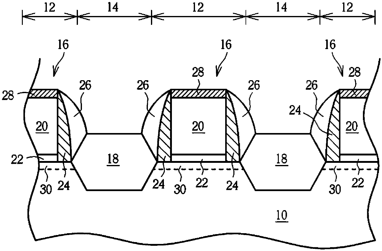
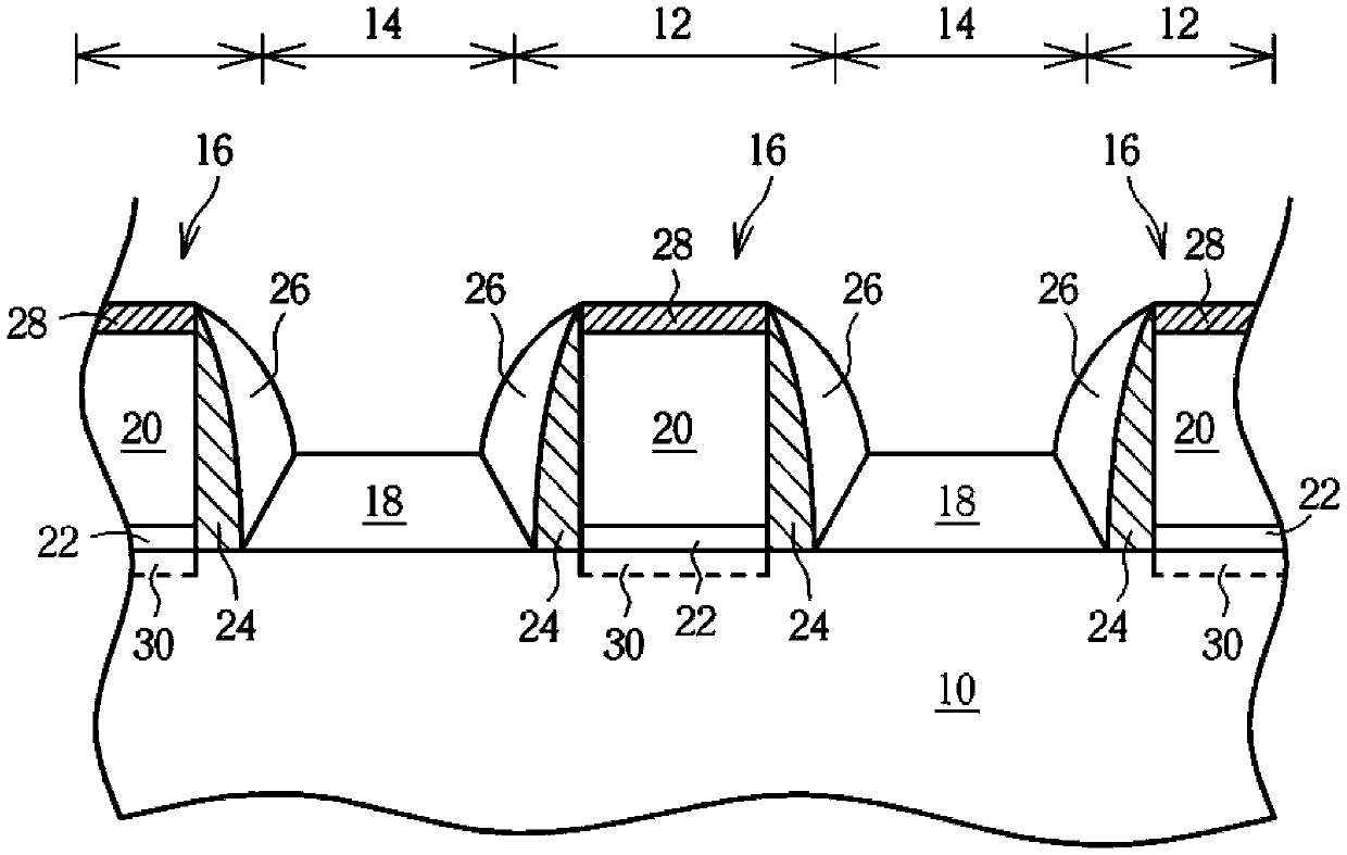
[0041] Please refer to figure 1 and figure 2 . figure 1 A simplified flowchart for preparing a semiconductor element according to the first embodiment of the present invention. figure 2 It is a schematic diagram of preparing a semiconductor element according to the first embodiment of the present invention. S...


PUM


Abstract

The invention discloses a semiconductor element and a manufacturing method thereof. The semiconductor element comprises a semiconductor substrate, a grid structure, at least one epitaxial layer, an interlayer dielectric layer, at least one contact hole, at least one metal silicide and a fluorine-containing layer. The semiconductor substrate is provided with at least one grid region and at least one source/drain region adjacent to the grid region. The grid structure is arranged in the grid region on the semiconductor substrate. The epitaxial layer is arranged in the source/drain region of the semiconductor substrate. The semiconductor substrate, the grid structure and the epitaxial layer are covered with the interlayer dielectric layer. The contact hole penetrates through the interlayer dielectric layer until the epitaxial layer is exposed outside . The metal silicide is located on the part, at the bottom of the contact hole, of the epitaxial layer. The fluorine-containing layer is arranged in or on the epitaxial layer and arranged on the periphery of a metal silicide layer.

Description

technical field [0001] The invention relates to a semiconductor element and a manufacturing method thereof, in particular to a semiconductor element with a fluorine-containing layer in the source / drain region and a manufacturing method thereof. Background technique [0002] As the integration level of integrated circuits (ICs) becomes higher and higher, the line width and geometric dimensions of semiconductor elements also step into sub-micron physical dimensions. Limited by the nature of the material, the increase in the degree of integration increases the junction resistance between the semiconductor layer and the external contact metal. Therefore, there is still a need to develop a semiconductor device with lower junction resistance to meet the needs of the industry. [0003] In the fabrication of the existing plug structure, a self-aligned silicon metallization process (self-aligned silicide, salicide) is generally used to form a metal silicide at the junction between t...

Claims


Application Information

Patent Timeline
Patent Type & Authority Applications(China)
IPC IPC(8): H01L29/78H01L29/06H01L21/336H01L29/423
CPCH01L29/0642H01L29/66795H01L29/785H01L29/7851H01L2029/7858
Inventor 陈意维黄建中刘国胜
Owner UNITED MICROELECTRONICS CORP
Why Eureka
Try Eureka