Infrared metamaterial wave absorbing body

A technology of wave absorber and infrared ultra-high, applied in the infrared field, can solve the problems of narrow tunable range, limit the wide application of infrared metamaterial wave absorbers, and reduce the absorption rate, and achieve the effect of ultra-high absorption rate

Inactive Publication Date: 2014-08-13
UNIV OF ELECTRONIC SCI & TECH OF CHINA
View PDF9 Cites 5 Cited by
  • Summary
  • Abstract
  • Description
  • Claims
  • Application Information

AI Technical Summary

Problems solved by technology

At present, the structure of the infrared metamaterial absorber that has been studied more is a cross structure. The infrared metamaterial absorber of this structure can achieve ultra-high absorption at a specific wavelength, but its tunable range is narrow, and when the i

Method used


Image

  • Infrared metamaterial wave absorbing body
  • Infrared metamaterial wave absorbing body
  • Infrared metamaterial wave absorbing body

Examples


Embodiment 1

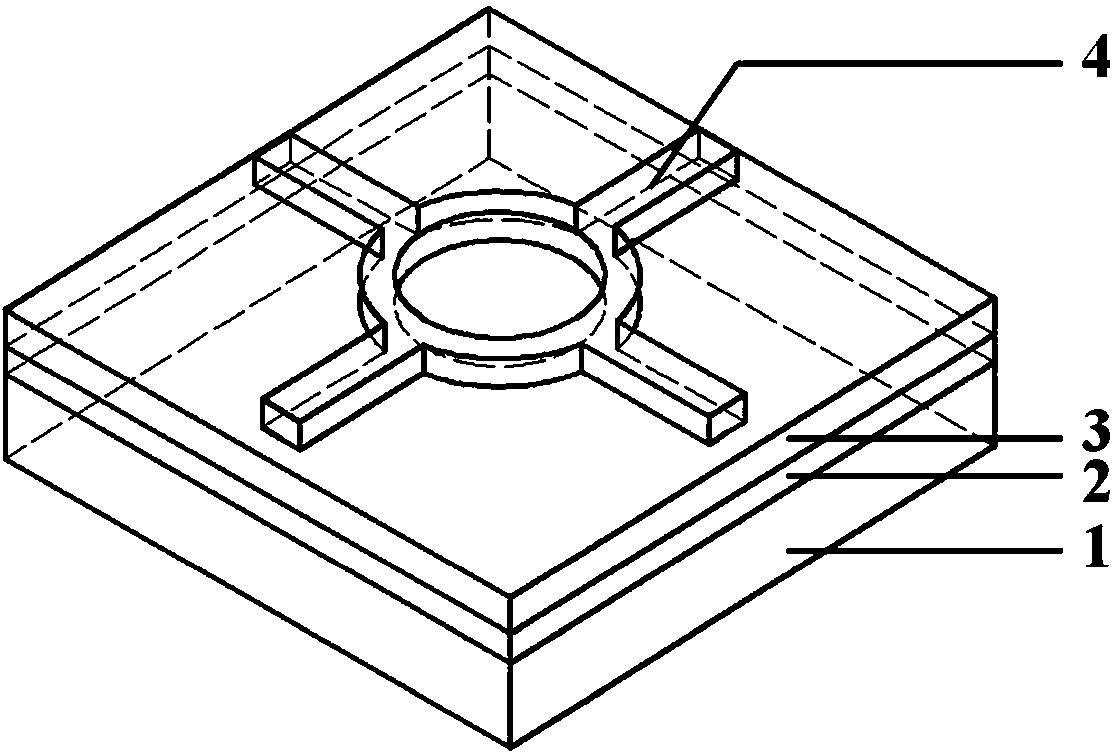
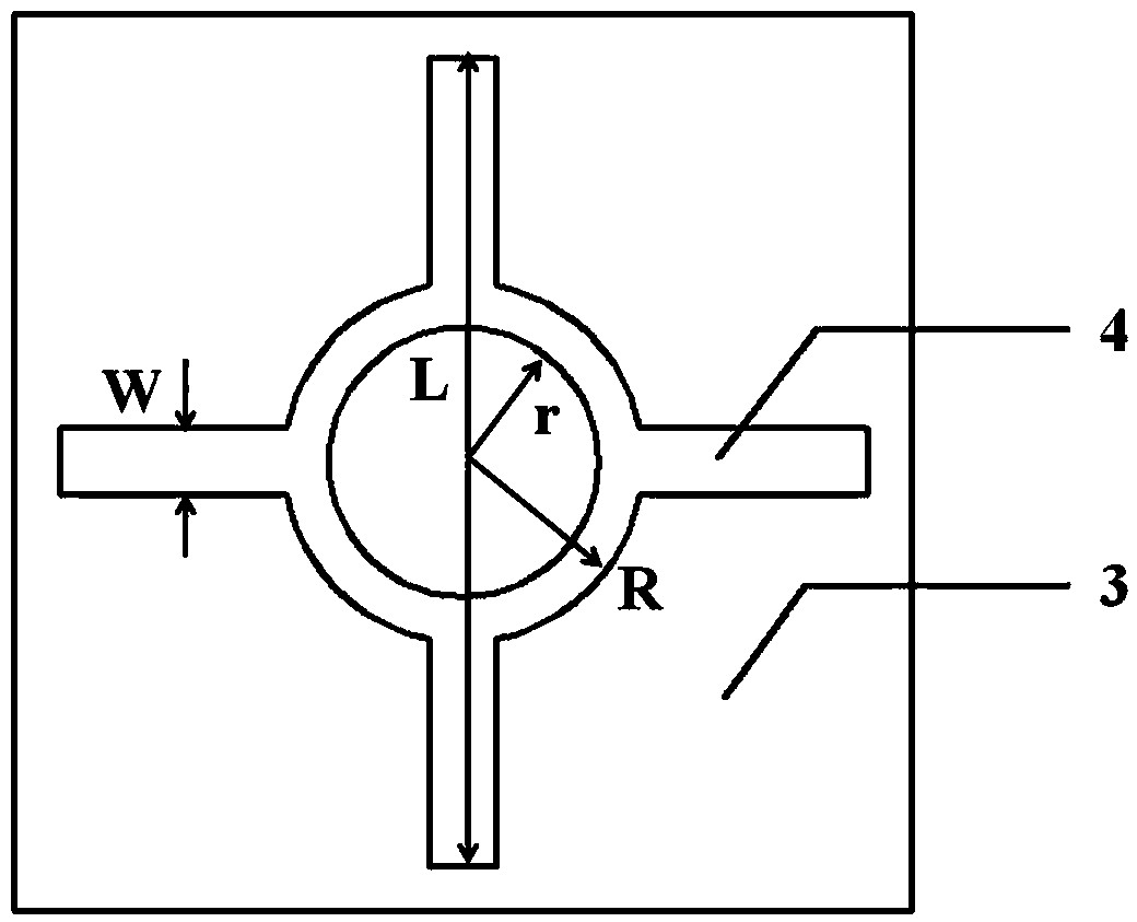
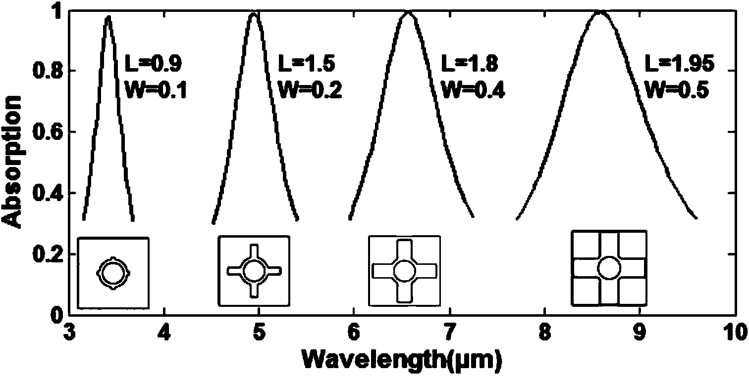
[0024] An infrared metamaterial absorber, the absorber uses four absorber units to form a 2×2 two-dimensional array structure, wherein each absorber unit includes a substrate 1, a metal layer 2, a dielectric layer 3 and a cross circle Ring structure 4. The upper and lower surfaces of the metal layer 2 are in contact with the lower surface of the dielectric layer 3 and the upper surface of the substrate 1 respectively. The substrate 1 is made of silicon material with a thickness of 50 microns; the metal layer 2 is located directly above the substrate 1 and is a continuous layer. The metal film is made of gold with a thickness of 0.1 micron; the dielectric layer 3 is located directly above the metal layer 2 and is made of magnesium fluoride with a thickness of 0.13 micron; the cross ring structure 4 is located directly above the dielectric layer 3 and is formed by A ring and a cross are intersected, and the cross part inside the ring is removed. The center of the ring coincides ...

Embodiment 2

[0026] An infrared metamaterial absorber, the absorber uses four absorber units to form a 2×2 two-dimensional array structure, wherein each absorber unit includes a substrate 1, a metal layer 2, a dielectric layer 3 and a cross circle Ring structure 4. The upper and lower surfaces of the metal layer 2 are in contact with the lower surface of the dielectric layer 3 and the upper surface of the substrate 1 respectively. The substrate 1 is made of silicon material with a thickness of 50 microns; the metal layer 2 is located directly above the substrate 1 and is a continuous layer. The metal film is made of gold with a thickness of 0.1 micron; the dielectric layer 3 is located directly above the metal layer 2 and is made of magnesium fluoride with a thickness of 0.13 micron; the cross ring structure 4 is located directly above the dielectric layer 3 and is formed by A ring and a cross are intersected, and the cross part inside the ring is removed. The center of the ring coincides ...

Embodiment 3

[0028] An infrared metamaterial absorber, the absorber uses four absorber units to form a 2×2 two-dimensional array structure, wherein each absorber unit includes a substrate 1, a metal layer 2, a dielectric layer 3 and a cross circle Ring structure 4. The upper and lower surfaces of the metal layer 2 are in contact with the lower surface of the dielectric layer 3 and the upper surface of the substrate 1 respectively. The substrate 1 is made of silicon material with a thickness of 50 microns; the metal layer 2 is located directly above the substrate 1 and is a continuous layer. The metal film is made of gold with a thickness of 0.1 micron; the dielectric layer 3 is located directly above the metal layer 2 and is made of magnesium fluoride with a thickness of 0.13 micron; the cross ring structure 4 is located directly above the dielectric layer 3 and is formed by A ring and a cross are intersected, and the cross part inside the ring is removed. The center of the ring coincides ...


PUM

PropertyMeasurementUnit
Thicknessaaaaaaaaaa
Thicknessaaaaaaaaaa
Inner radiusaaaaaaaaaa

Abstract

The invention provides an infrared metamaterial wave absorbing body. The infrared metamaterial wave absorbing body comprises at least four wave absorbing body units arranged in a matrix mode. Each wave absorbing body unit comprises a substrate, a metal layer located right above the substrate, a dielectric layer located right above the metal layer and a cross round ring structure located right above the dielectric layer, wherein the cross round ring structure is attached to the surface of the dielectric layer and formed by crossing a round ring and a cross and then removing the cross part in the round ring, the circle center of the round ring and the geometric center of the cross coincide, and the cross part outside the round ring forms four arms of the cross round ring structure. The lengths of the four arms of the cross round ring structure are the same, the widths of the four arms of the cross round ring structure are the same, the cross sections of the substrate, the metal layer and the dielectric layer are all square, and the arms of the cross round ring structure are parallel with one edge of each square. The infrared metamaterial wave absorbing body is high in absorbing rate, wide in incidence angle and insensitive in polarization, and has good tunability.

Description

technical field [0001] The invention belongs to the field of infrared technology, and in particular relates to an infrared metamaterial absorber. Background technique [0002] Infrared absorbing materials refer to special functional materials that have strong absorption for a certain frequency band or several frequency bands in the infrared region, and are the key to the preparation of high-performance infrared sensors. Traditional infrared absorbing materials mainly use the energy level transition of the material to convert electromagnetic energy into molecular potential energy, electronic potential energy, etc. inside the material. The conversion efficiency will be limited by the material, and it is difficult to achieve ultra-high infrared absorption. As a new type of electromagnetic absorption structure, metamaterial absorbers can achieve near-perfect absorption of electromagnetic waves based on electromagnetic coupling. [0003] As a new artificial electromagnetic mater...

Claims


Application Information

Patent Timeline
IPC IPC(8): G02B5/00
Inventor 顾德恩侯剑章郭瑞王志辉王涛袁凯蒋亚东
Owner UNIV OF ELECTRONIC SCI & TECH OF CHINA
Why Eureka
Try Eureka