Multispectral transparent microwave absorbing material and preparation method thereof
A microwave absorbing material and multi-spectral technology, applied in the field of multi-spectral transparent microwave absorbing materials and its preparation, can solve the problems that window glass cannot achieve optical transparency and microwave shielding, absorption compatibility, etc.
- Summary
- Abstract
- Description
- Claims
- Application Information
AI Technical Summary
Problems solved by technology
Method used
Image
Examples
preparation example Construction
[0056] In a second aspect, the present invention provides a method for preparing the multi-spectral transparent microwave absorbing material provided in the first aspect of the present invention, the preparation method comprising the following steps:
[0057] (1) a step of plating a surface layer periodic metal grid on the upper surface of the optical window by photolithography; and
[0058] (2) A step of plating the underlying periodic metal grid on the lower surface of the optical window by using a photolithography process.
[0059] It should be noted that the change in the order of step (1) and step (2) will not affect the preparation method.
[0060] In some preferred embodiments, the step (1) is carried out as follows:
[0061] Coating photosensitive adhesive on the surface of the optical window, using a mask plate prefabricated according to the pattern of the periodic metal grid on the surface for pattern exposure, and then developing, and then using vacuum magnetron sput...
Embodiment 1
[0069] The multi-spectral transparent microwave absorbing material provided in this embodiment is composed of a periodic metal grid on the surface, an optical window, and a periodic metal grid on the bottom layer, and has a three-layer structure, such as figure 1 As shown, the optical window is located in the middle, the surface periodic metal grid is formed on the upper surface, and the bottom layer periodic metal grid is formed on the lower surface.
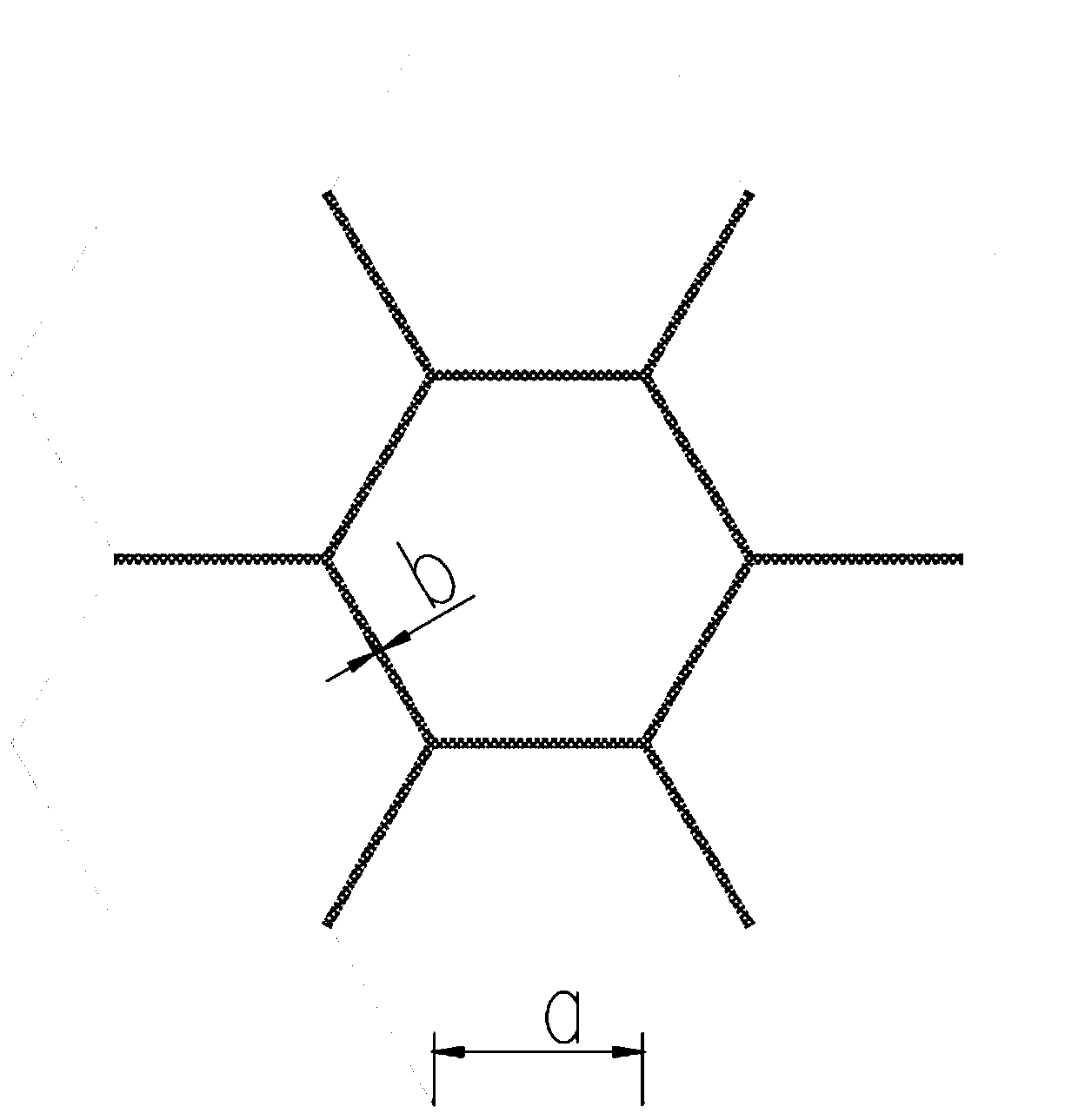
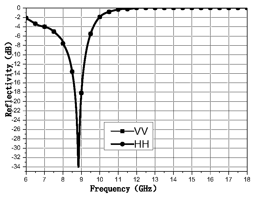
[0070] From top to bottom, the first layer is the surface periodic metal grid, thickness d1=0.05mm, the second layer is the optical window, the material is quartz glass, thickness d2=5mm, the third layer is the bottom periodic metal grid, thickness d1 = 0.05 mm. Among them, the surface periodic metal grid is plated on the upper surface of the optical window glass by photolithography. The periodic structural unit is a regular hexagon. The structural unit and periodic form are as follows: figure 2 As shown, side length a=4mm, l...
Embodiment 2
[0080] The multi-spectral transparent microwave absorbing material provided in this embodiment is composed of a periodic metal grid on the surface, an optical window, and a periodic metal grid on the bottom layer, and has a three-layer structure, such as figure 1 As shown, the optical window is located in the middle, the surface periodic metal grid is formed on the upper surface, and the bottom layer periodic metal grid is formed on the lower surface.
[0081] From top to bottom, the first layer is the surface periodic metal grid, thickness d1=0.05mm, the second layer is optical window glass, the material is quartz glass, thickness d2=3mm, the third layer is the bottom periodic metal grid, thickness d1 = 0.05mm. Among them, the surface periodic metal grid is plated on the upper surface of the optical window glass by photolithography. The periodic structural unit is a regular hexagon. The structural unit and periodic form are as follows: figure 2 As shown, a=5mm, b=0.08mm. T...
PUM
| Property | Measurement | Unit |
|---|---|---|
| thickness | aaaaa | aaaaa |
| width | aaaaa | aaaaa |
| thickness | aaaaa | aaaaa |
Abstract
Description
Claims
Application Information


