Method for improving exposure shape of photoresist and method for patterning semiconductor substrate

A patterning and semiconductor technology, which is applied in the field of patterning semiconductor substrates and improving the exposure morphology of photoresist, can solve the problems affecting the quality of lithography process, the quality of substrate or film layer, etc., and achieve the improvement of exposure quality and lithography Workmanship quality, avoiding collapse defects, and improving the effect of workmanship quality

Inactive Publication Date: 2014-08-13
SHANGHAI HUALI MICROELECTRONICS CORP
View PDF12 Cites 0 Cited by
  • Summary
  • Abstract
  • Description
  • Claims
  • Application Information

AI Technical Summary

Problems solved by technology

[0003] The collapse defects caused by the inverted trapezoidal photoresist not only affect the quality of the photolithography process, but also affect the quality of the patterned substrate or thin film layer using the photolithography and etching process

Method used


Image

  • Method for improving exposure shape of photoresist and method for patterning semiconductor substrate
  • Method for improving exposure shape of photoresist and method for patterning semiconductor substrate
  • Method for improving exposure shape of photoresist and method for patterning semiconductor substrate

Examples


Embodiment Construction

[0026] In order to make the content of the present invention clearer and easier to understand, the content of the present invention will be further described below in conjunction with the accompanying drawings. Of course, the present invention is not limited to this specific embodiment, and general replacements known to those skilled in the art are also covered within the protection scope of the present invention.

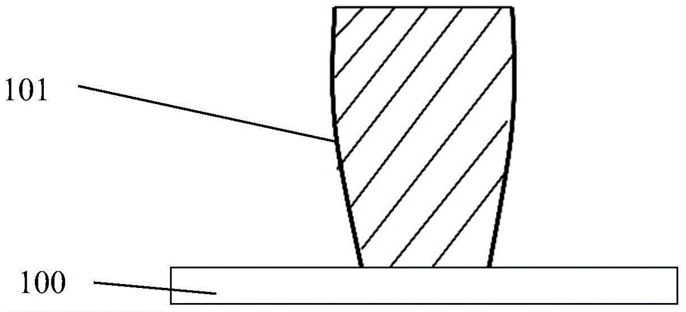
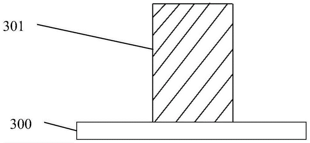
[0027] As mentioned above, the thickness of the photoresist on the thicker metal layer is thicker, and because of the higher reflectivity of the semiconductor substrate surface, it is easy to form an inverted trapezoidal photoresist topography after exposure. Photoresists are prone to collapse defects. For this reason, the present invention adopts the method of forming a composite thin film layer on the surface of the semiconductor substrate, because the composite thin film layer has a relatively low surface reflectivity, thereby avoiding the occurrence of the abov...


PUM

PropertyMeasurementUnit
temperatureaaaaaaaaaa
thicknessaaaaaaaaaa
thicknessaaaaaaaaaa

Abstract

The invention provides a method for improving the exposure shape of a photoresist and a method for patterning a semiconductor substrate. The method for improving the exposure shape of the photoresist comprises the following steps: depositing a composite film layer on the surface of the semiconductor substrate, wherein the surface of the composite film layer has low reflectivity; coating the composite film layer with the photoresist; and exposing and developing the photoresist, so as to pattern the photoresist. According to the methods, by utilizing the characteristic that the surface of the composite film layer has low reflectivity, the photoresist cannot form an inverted trapezoidal shape in an exposure process, so that a collapse defect of the photoresist is avoided, the exposure quality and the photolithographic process quality are improved, and the quality of the process for subsequently patterning the semiconductor substrate is improved.

Description

technical field [0001] The invention relates to the technical field of semiconductors, in particular to a method for improving the exposure profile of a photoresist and a method for patterning a semiconductor substrate. Background technique [0002] The photolithography process includes: coating photoresist on the substrate, exposing and developing the photoresist, and baking the photoresist. The thickness of the photoresist on the thicker metal layer is thicker, and it is easy to form an inverted trapezoidal photoresist topography after exposure. Please refer to figure 1 , figure 1 It is a schematic structural diagram of an inverted trapezoidal photoresist, wherein 101 is an inverted trapezoidal photoresist, and 100 is a substrate. For a photoresist with a large photoresist length, it is easy to cause collapse defects. The thinner the size of the photoresist, the easier it is for the photoresist to collapse. The formation of the inverted trapezoidal photoresist is mainl...

Claims


Application Information

Patent Timeline
Patent Type & Authority Applications(China)
IPC IPC(8): G03F7/20H01L21/027
Inventor 魏娟徐炯周维魏峥颖
Owner SHANGHAI HUALI MICROELECTRONICS CORP
Why Eureka
Try Eureka