Wafer-level packaging method for semiconductor and semiconductor packaging part

A wafer-level packaging and semiconductor technology, applied in the fields of semiconductor devices, semiconductor/solid-state device manufacturing, electric solid-state devices, etc., can solve the problem of the narrow application range of wafer-to-wafer packaging, and improve the scope of packaging and reduce the area. wasteful effect

Active Publication Date: 2014-08-13
GALAXYCORE SHANGHAI
View PDF4 Cites 10 Cited by
  • Summary
  • Abstract
  • Description
  • Claims
  • Application Information

AI Technical Summary

Problems solved by technology

However, the application range of wafer

Method used


Image

  • Wafer-level packaging method for semiconductor and semiconductor packaging part
  • Wafer-level packaging method for semiconductor and semiconductor packaging part
  • Wafer-level packaging method for semiconductor and semiconductor packaging part

Examples


Embodiment Construction

[0045] As mentioned in the background art, the current wafer-to-wafer packaging is still very narrow in application. One type of memory wafer cannot adapt to logic wafers of different sizes, and generally can only be used for one type of logic wafer.

[0046] To this end, the present invention provides a new semiconductor wafer-level packaging method, which improves the application range of wafer-to-wafer packaging by matching one logic chip unit with more than one memory chip unit, and Reduce the waste of chip area.

[0047] In order to make the above objects, features and advantages of the present invention more comprehensible, specific embodiments of the present invention will be described in detail below in conjunction with the accompanying drawings.

[0048] An embodiment of the present invention provides a semiconductor wafer-level packaging method, please refer to Figure 1 to Figure 4 .

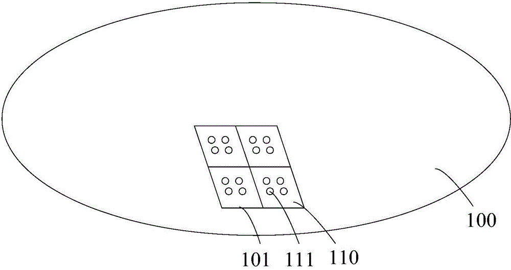
[0049] Please refer to figure 1 , providing a first wafer 100 having one or mo...


PUM


Abstract

Provided are a wafer-level packaging method for a semiconductor and a semiconductor packaging part. The wafer-level packaging method for the semiconductor comprises the following steps that a first wafer with one or a plurality of storage chip units is provided, each storage chip unit is provided with a storage array circuit and a periphery circuit, and a first cut channel is arranged between the adjacent storage chip units; a second wafer provided with one or more logical chip units is provided, the area of each logical chip unit corresponds to the area of N storage chip units, wherein N is a natural number larger than or equal to 1, a second cut channel is arranged between the adjacent logical chip units, and the second cut channels are matched with the first cut channels on the peripheries of the N storage chip units; the first wafer and the second wafer are bonded, and the logical chip units are correspondingly matched with the N storage chip units. By means of the wafer-level packaging method, the packaging application range of the storage wafers is enlarged.

Description

technical field [0001] The invention relates to the field of semiconductor manufacturing, in particular to a semiconductor wafer-level packaging method and a semiconductor package. Background technique [0002] There are many kinds of memory, such as Static Random Access Memory (SRAM), Dynamic Random Access Memory (DRAM), Flash Memory (FLASH), Phase Change Memory (Phase Change Memory, PCM), etc., they are widely It is used in various electronic devices and occupies an important position in the circuit. [0003] A logic chip generally refers to a chip with a programmable logic device (PLD), and the logic chip has a high degree of integration, which is sufficient to meet the needs of designing a general digital system. [0004] Currently, there are generally the following methods for connecting memory chips and logic chips: [0005] 1. The two bare chips are packaged separately, and after completion, they are soldered on the circuit board and connected by circuit board trace...

Claims


Application Information

Patent Timeline
IPC IPC(8): H01L21/60H01L25/16
CPCH01L24/82H01L25/18H01L2224/82
Inventor 赵立新
Owner GALAXYCORE SHANGHAI
Why Eureka
Try Eureka