TFT array substrate and manufacturing method thereof
A technology for array substrates and manufacturing methods, applied in the field of flat panel displays, capable of solving problems such as low mobility and lengthy process
- Summary
- Abstract
- Description
- Claims
- Application Information
AI Technical Summary
Problems solved by technology
Method used
Image


Examples
Embodiment 1
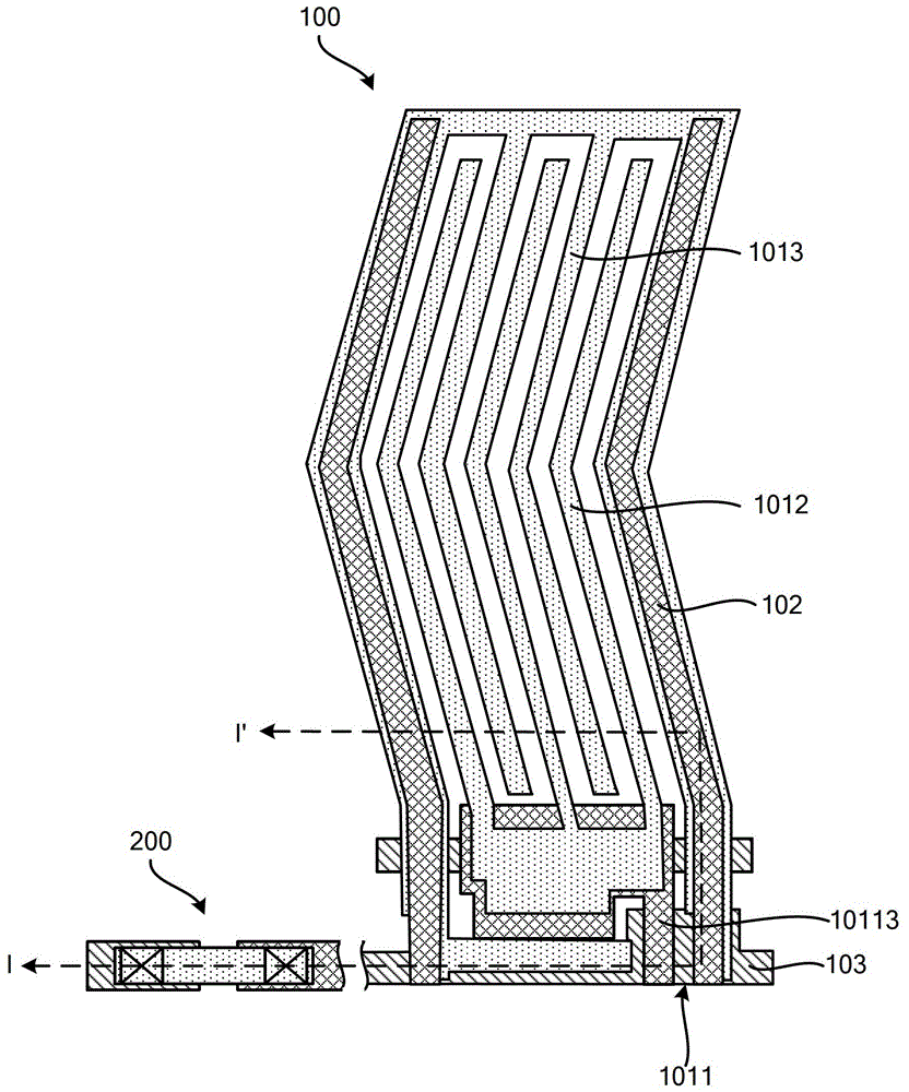
[0085] image 3 It is a top view of the TFT array substrate of this embodiment. Such as image 3 As shown, the TFT array substrate 200 of this embodiment includes a substrate 201 , and the substrate 201 includes a plurality of pixel structures 202 and line switching structures 203 . The pixel structure 202 includes a TFT 2021 , scan lines 2022 and data lines 2023 .
[0086] Such as Figure 4 As shown, the TFT 2021 includes a gate 20211 , a gate insulating layer 20212 , a semiconductor active layer 20213 and a source / drain 20214 . In addition, the pixel 202 further includes a pixel electrode 2022 , a passivation layer 2023 and a common electrode 2024 . The gate 20211 is formed on the substrate 201, the gate insulating layer 20212 is formed on the gate 20211, the semiconductor active layer 20213 is formed on the gate insulating layer 20212, the source The electrode / drain 20214 is formed on the gate insulating layer 20212 and overlaps part of the semiconductor active layer 2...
Embodiment 2
[0118] The difference between this embodiment and Embodiment 1 lies in that the compound semiconductor layer as the semiconductor layer is formed by two sputtering depositions instead of hydrogen ion implantation.
[0119] Specifically, the formation process of the compound semiconductor layer is as follows:
[0120] Using a physical vapor deposition method, sputtering a first target material to deposit on the substrate to form a first semiconductor layer; then, sputtering a second target material to deposit on the first semiconductor layer to form a second semiconductor layer. Wherein, both the first target material and the second target material are transparent metal oxide targets, and the ion oxide concentration of the second target material is higher than that of the first target material. Preferably, the thickness of the semiconductor layer is The thickness of the first semiconductor layer is The thickness of the second semiconductor layer is 500
[0121] By adopti...
Embodiment 3
[0123] The difference between this embodiment and Embodiment 1 is that the semiconductor layer is a single-layer semiconductor layer, which is different from the composite semiconductor layer in Embodiment 1 and Embodiment 2.
[0124] Such as Figure 16 As shown, the TFT 2021 includes a gate 20211 , a gate insulating layer 20212 , a semiconductor active layer 20213 , a source / drain 20214 , a pixel electrode 2022 , a passivation layer 2023 and a common electrode 2024 . Wherein, the semiconductor active layer 20213 and the pixel electrode 2022 are formed by the same semiconductor layer 20218, and the semiconductor layer 20218 is a single-layer semiconductor layer. In order to ensure the conductivity of the pixel electrode 2022 and the semiconductor performance of the semiconductor active layer 20213, the thickness of the semiconductor active layer 20213 can be made smaller than the thickness of the pixel electrode 2022, and the residual metal ions sputtered on the surface of the...
PUM
 Abstract
Description
Claims
Application Information
 - R&D
- Intellectual Property
- Life Sciences
- Materials
- Tech Scout
- Unparalleled Data Quality
- Higher Quality Content
- 60% Fewer Hallucinations
Browse by: Latest US Patents, China's latest patents, Technical Efficacy Thesaurus, Application Domain, Technology Topic, Popular Technical Reports.
© 2025 PatSnap. All rights reserved.Legal|Privacy policy|Modern Slavery Act Transparency Statement|Sitemap|About US| Contact US: help@patsnap.com