Method for manufacturing display device, repairing method and liquid crystal display panel

A display device and substrate technology, which is applied in the field of liquid crystal display panels and display devices of liquid crystal displays, can solve problems such as broken data lines, lower pass rate of liquid crystal display panels, and difficulty in repairing, so as to reduce difficulty, improve display quality, and improve finished products rate effect

Active Publication Date: 2014-08-20
TCL CHINA STAR OPTOELECTRONICS TECH CO LTD
View PDF5 Cites 2 Cited by
  • Summary
  • Abstract
  • Description
  • Claims
  • Application Information

AI Technical Summary

Problems solved by technology

Data lines are prone to breakage and are difficult to repair, which reduces the yield of LCD panels

Method used


Image

  • Method for manufacturing display device, repairing method and liquid crystal display panel
  • Method for manufacturing display device, repairing method and liquid crystal display panel
  • Method for manufacturing display device, repairing method and liquid crystal display panel

Examples


Embodiment Construction

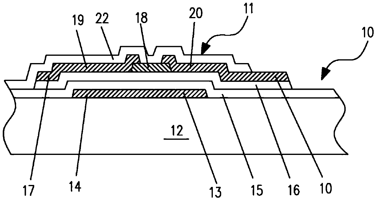
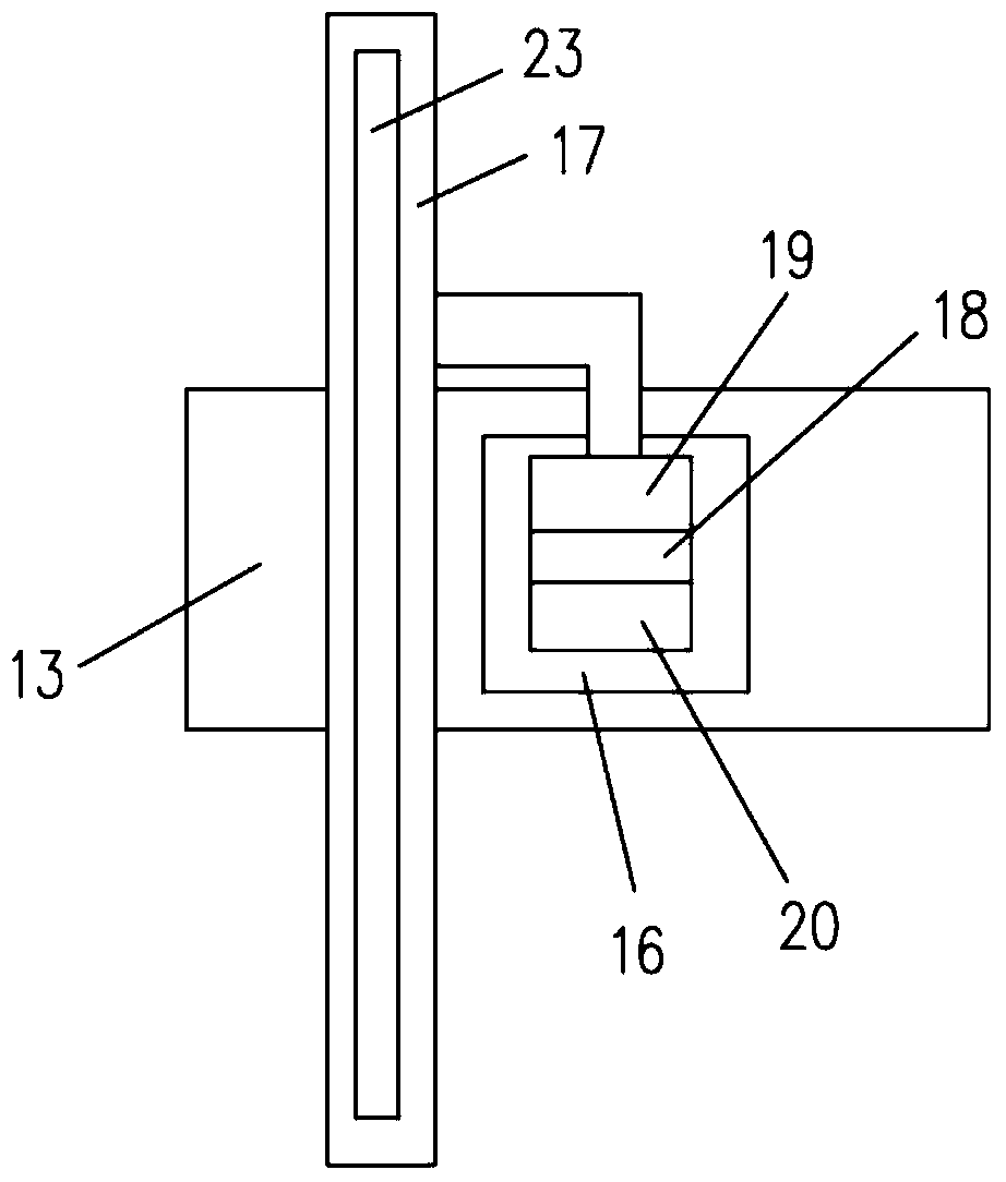
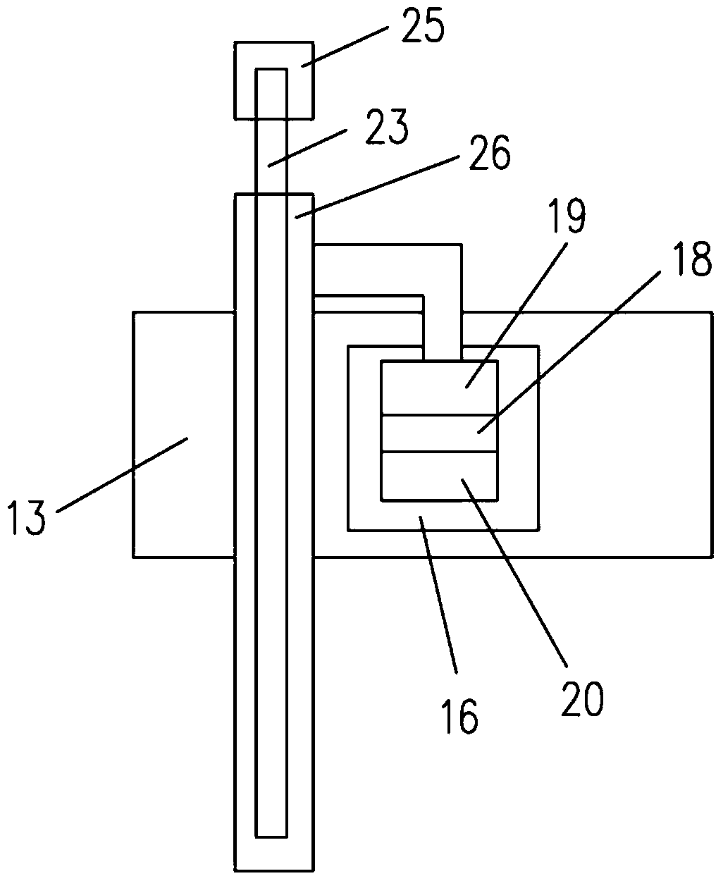
[0026] The present invention will be further described below in conjunction with accompanying drawing.

[0027] figure 1 A schematic view of the layered structure of the display device 10 according to the present invention is schematically shown. A thin film transistor 11 is provided on the display device 10 . The thin film transistor 11 is a common switching element in the field of liquid crystal display, and its arrangement in the display device 10 is well known to those skilled in the art, and will not be repeated here. Here, the method for manufacturing the thin film transistor 11 will be mainly described.

[0028] Fabricating the thin film transistor 11 includes the following steps.

[0029] Firstly, the gate 13 and the scanning line 14 are arranged on the substrate 12, then the first insulating layer 15 is arranged on the gate 13 and the scanning line 14, and then the semiconductor layer 16 is arranged on the first insulating layer 15, wherein the semiconductor layer ...


PUM

PropertyMeasurementUnit
wavelengthaaaaaaaaaa

Abstract

The invention relates to a method for manufacturing a display device, a repairing method and a liquid crystal display panel. The method for manufacturing the display device comprises the steps that firstly, a grid electrode, a scanning line, a first insulating layer and a semiconductor layer are sequentially arranged on a substrate; secondly, the position of a data line is determined on the semiconductor layer, and an etching preventing layer is arranged at the position, deviating from the data line, on the semiconductor layer; thirdly, the part, in the position of the data line, of the semiconductor layer is modified into a conductor; fourthly, a source electrode, a drain electrode, the data line and a second insulating layer are arranged on the semiconductor layer. According to the repairing method, when the data line is broken, broken data line segments are connected with a conductor layer below the data line respectively in a melting mode. The display device manufactured through the method is high in display quality and easy to repair.

Description

technical field [0001] The invention relates to a display device, especially a display device for liquid crystal display. The present invention also relates to a repair method of the display device, and a liquid crystal display panel including the display device. Background technique [0002] Generally, a liquid crystal display panel includes a display substrate, an opposite substrate facing the display substrate, and a liquid crystal layer interposed between the display substrate and the opposite substrate. The display substrate includes switching elements and pixel electrodes. A voltage is applied to the liquid crystal layer to control the transmittance of light through the liquid crystal layer, thereby displaying an image. [0003] In the prior art, the switching element is usually a thin film transistor, the source of the thin film transistor is connected to the data line, and the drain is connected to the pixel electrode. Data lines are prone to breakage and are diff...

Claims


Application Information

Patent Timeline
Patent Type & Authority Applications(China)
IPC IPC(8): G02F1/1333G02F1/1362G02F1/1368G02F1/13
CPCG02F1/136259G02F1/136263
Inventor 郑扬霖
Owner TCL CHINA STAR OPTOELECTRONICS TECH CO LTD
Why Eureka
Try Eureka