Light-emitting diode epitaxial wafer and growth method thereof

A technology of light-emitting diodes and epitaxial wafers, which is applied in the direction of semiconductor devices, electrical components, circuits, etc., and can solve the problems that the crystal quality of epitaxial wafers and LED operating voltage cannot be taken into account at the same time

Active Publication Date: 2020-07-07
HC SEMITEK ZHEJIANG CO LTD
View PDF4 Cites 0 Cited by
  • Summary
  • Abstract
  • Description
  • Claims
  • Application Information

AI Technical Summary

Problems solved by technology

[0006] The embodiment of the present invention provides a light-emitting diode epitaxial wafer and its growth method, which can solve the problem that the existing technology cannot take into account both the crystal quality of the epitaxial wafer and the LED operating voltage.

Method used


Image

  • Light-emitting diode epitaxial wafer and growth method thereof
  • Light-emitting diode epitaxial wafer and growth method thereof
  • Light-emitting diode epitaxial wafer and growth method thereof

Examples


Embodiment Construction

[0030] In order to make the object, technical solution and advantages of the present invention clearer, the implementation manner of the present invention will be further described in detail below in conjunction with the accompanying drawings.

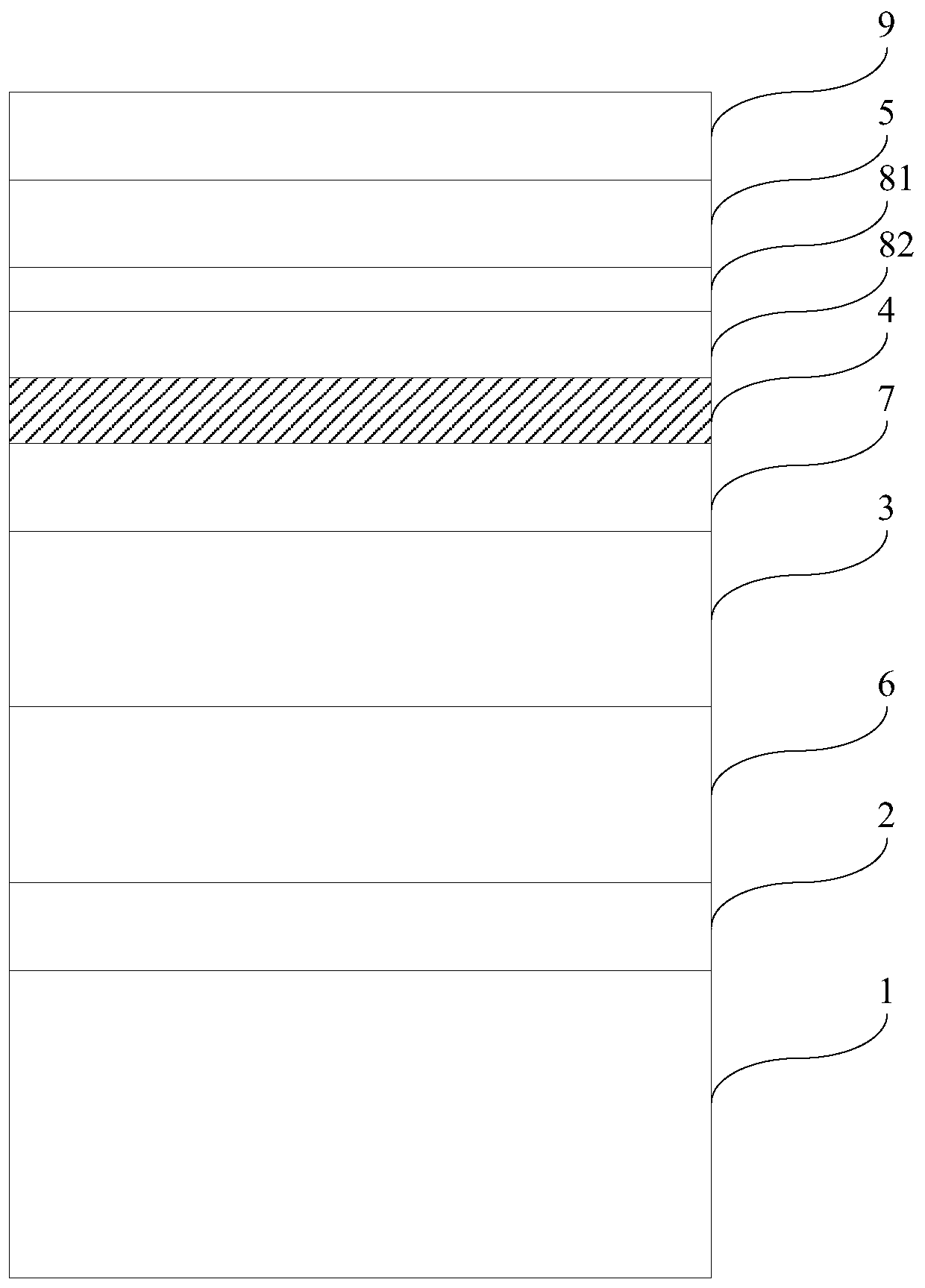
[0031] An embodiment of the present invention provides a light emitting diode epitaxial wafer. figure 1 A schematic structural diagram of a light emitting diode epitaxial wafer provided by an embodiment of the present invention. see figure 1, the light-emitting diode epitaxial wafer includes a substrate 1, a buffer layer 2, an N-type semiconductor layer 3, an active layer 4, and a P-type semiconductor layer 5, and the buffer layer 2, the N-type semiconductor layer 3, the active layer 4, and the P-type semiconductor layer Layers 5 are sequentially stacked on the substrate 1 .

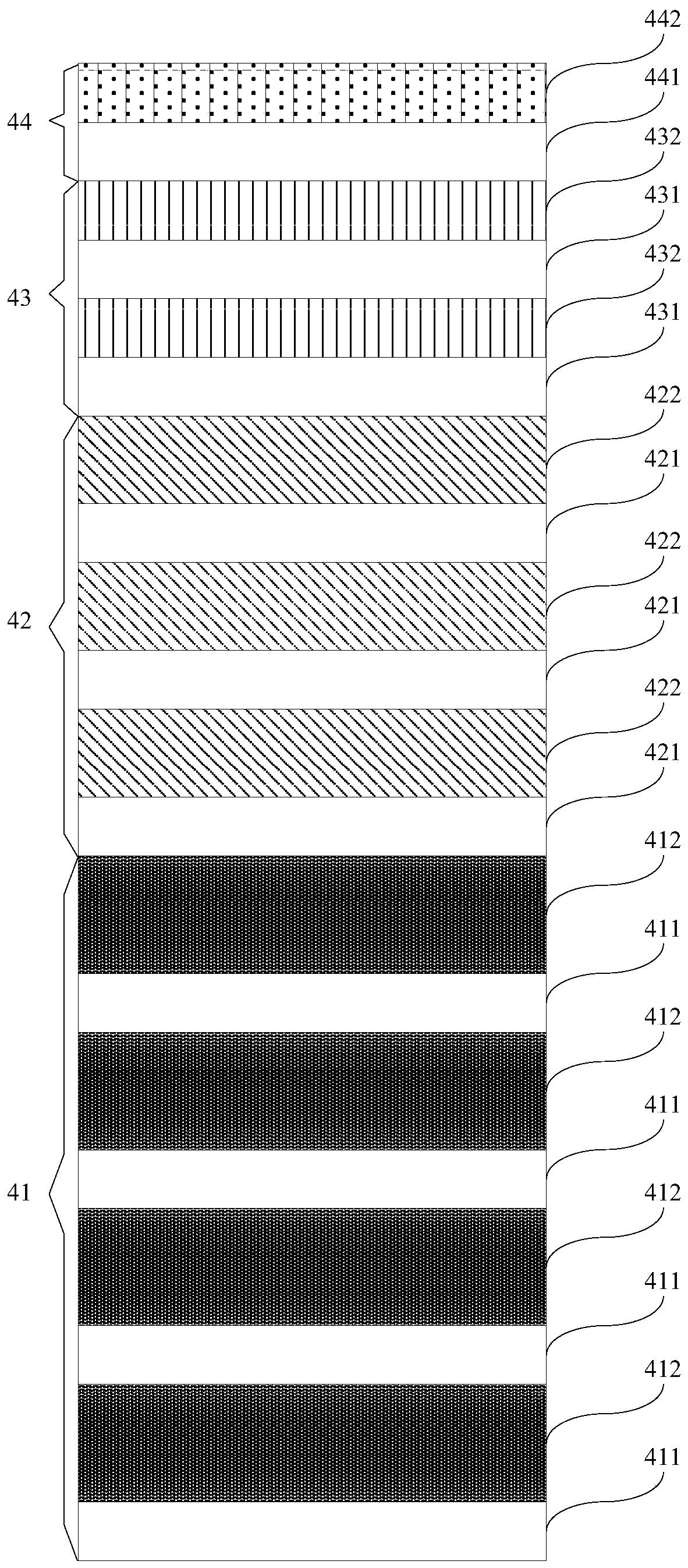
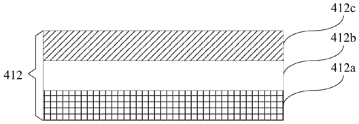
[0032] figure 2 A schematic structural diagram of an active layer provided by an embodiment of the present invention. see figure 2 , the active layer 4 in...


PUM

PropertyMeasurementUnit
thicknessaaaaaaaaaa
thicknessaaaaaaaaaa
thicknessaaaaaaaaaa

Abstract

The invention discloses a light-emitting diode epitaxial wafer and a growing method thereof and belongs to the field of semiconductor technology. The epitaxial wafer comprises a substrate, a buffer layer, an N-type semiconductor layer, an active layer and a P-type semiconductor layer, wherein the active layer comprises a first stacked structure, a second stacked structure, a third stacked structure and a fourth stacked structure; a quantum barrier of the first stacked structure comprises a first sub-layer, a second sub-layer and a third sub-layer, and a quantum barrier of the second stacked structure comprises a fourth sub-layer and a fifth sub-layer; materials of the first sub-layer, the third sub-layer, the fourth sub-layer and a quantum barrier of the fourth stacked structure are all undoped gallium nitride, and materials of the second sub-layer, the fifth sub-layer and a quantum barrier of the third stacked structure are all silicon-doped gallium nitride; and the average doping concentration of silicon in the quantum barrier of the first stacked structure, the average doping concentration of silicon in the quantum barrier of the second stacked structure and the doping concentration of silicon in the third stacked structure are gradually reduced. Through the light-emitting diode epitaxial wafer, radiation recombination efficiency is improved finally.

Description

technical field [0001] The invention relates to the technical field of semiconductors, in particular to a light-emitting diode epitaxial wafer and a growth method thereof. Background technique [0002] A light-emitting diode (English: Light Emitting Diode, referred to as: LED) is a semiconductor electronic component that can emit light. As an efficient, environmentally friendly, and green new solid-state lighting source, LEDs are rapidly and widely used in traffic lights, automotive interior and exterior lights, urban landscape lighting, mobile phone backlights and other fields. The core component of LED is the chip, and improving the luminous efficiency of the chip is the goal that is constantly pursued in the process of LED application. [0003] The chip includes an epitaxial wafer and electrodes provided on the epitaxial wafer. The existing LED epitaxial wafer includes a substrate, a buffer layer, an N-type semiconductor layer, an active layer and a P-type semiconductor...

Claims


Application Information

Patent Timeline
Patent Type & Authority Patents(China)
IPC IPC(8): H01L33/00H01L33/02H01L33/06
Inventor 姚振从颖胡加辉李鹏
Owner HC SEMITEK ZHEJIANG CO LTD
Why Eureka
Try Eureka