Gallium nitride-based light-emitting diode and preparation method thereof

A light-emitting diode, GaN-based technology, used in semiconductor devices, electrical components, circuits, etc., can solve problems such as unfavorable productivity, lattice mismatch, time effects, etc., to improve EfficiencyDroop, shorten program time, reduce The effect of heating and cooling time

Active Publication Date: 2017-10-20
ANHUI SANAN OPTOELECTRONICS CO LTD
View PDF7 Cites 0 Cited by
  • Summary
  • Abstract
  • Description
  • Claims
  • Application Information

AI Technical Summary

Problems solved by technology

However, the luminous efficiency of LED is relatively low at present. From the perspective of epitaxial structure, further improving the electron hole injection efficiency and recombination efficiency in the active layer of LED needs to improve the internal quantum efficiency (IQE: Internal Quantum Efficiency)
[0003] The traditional multi-quantum well active layer is composed of GaN quantum barriers and InGaN quantum well structures. However, due to the lattice mismatch between GaN and InGaN materials, the polarization effect occurs, causing the conduction band and the valence band to be discontinuous, resulting in a light-emitting device. The phenomenon that the internal quantum efficiency declines with the increase of the applied current density intensifies, resulting in Efficiency Droop, which affects the quality and application range of the device
[0004] In addition, in the traditional multi-quantum well active layer structure, there is a large temperature difference between the well and the barrier, and there is a long heating and cooling time during the growth process, which has a certain impact on the entire process time, which is not conducive to the improvement of production capacity.

Method used


Image

  • Gallium nitride-based light-emitting diode and preparation method thereof
  • Gallium nitride-based light-emitting diode and preparation method thereof
  • Gallium nitride-based light-emitting diode and preparation method thereof

Examples


Embodiment Construction

[0019] Specific embodiments of the present invention will be described in detail below in conjunction with the accompanying drawings.

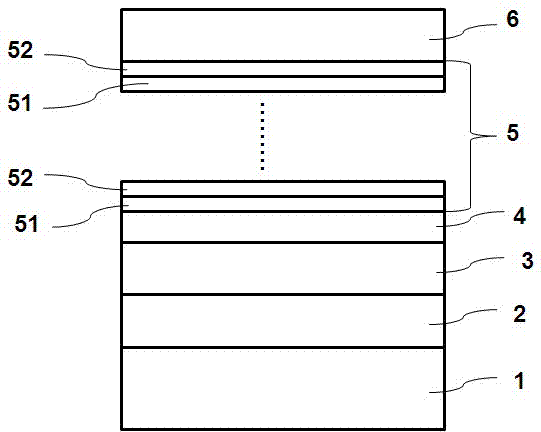
[0020] Please see attached figure 1 , a gallium nitride-based light-emitting diode generally includes: a substrate 1, a buffer layer 2, an N-type layer 3, a stress release layer 4, a multi-quantum well active region 5, and a P-type layer 6 from bottom to top. The manufacturing method of the foregoing light-emitting diode includes steps: 1) growing a buffer layer 2 on a substrate 1; 2) growing an N-type layer 3 on the buffer layer 2; 3) growing a stress release layer 4 on the N-type layer 3; 4) Growing a multi-quantum well active region 5 on the stress release layer 4; 6) growing a P-type layer 6 on the multi-quantum well active region 5.

[0021] Specifically, the material of the substrate 1 can be aluminum oxide single crystal (Sapphire), SiC (6H-SiC or 4H-SiC), Si, GaAs, GaN substrate or a single crystal oxide whose lattice constant is clos...


PUM


Abstract

The invention discloses a GaN-based light-emitting diode which comprises a substrate, a buffer layer, an N-type layer, a multiple quantum well active layer and a P-type layer, wherein the multiple quantum well active layer consists of InGaN quantum wells and InAlN quantum barriers. In the GaN-based light-emitting diode, InAlN materials in lattice matching with InGaN quantum well materials serve as the quantum barriers, so that a QCSE (Quantum-Confined Stark Effect) is improved, Efficiency Droop of a device is improved, the light-emitting efficiency of the device is improved, and IQE (Internal Quantum Efficiency) of an LED (Light-Emitting Diode) assembly is improved.

Description

technical field [0001] The invention relates to the field of semiconductor photoelectric device preparation, in particular to a gallium nitride-based light-emitting diode and a preparation method thereof. Background technique [0002] Light-emitting diodes (Light-emitting diodes, LEDs) are widely concerned due to their advantages in energy saving, environmental protection and long lifespan. In particular, LEDs based on gallium nitride materials have become the mainstream direction of LED development because their wavelength range theoretically covers the entire visible light band and ultraviolet band. Gallium nitride blue LED technology has made progress in both research and commercial production applications, and its application fields are broad. However, the luminous efficiency of LED is relatively low at present. From the perspective of epitaxial structure, further improving the electron hole injection efficiency and recombination efficiency in the LED active layer needs...

Claims


Application Information

Patent Timeline
Patent Type & Authority Patents(China)
IPC IPC(8): H01L33/06H01L33/32H01L33/00
CPCH01L33/06H01L33/32
Inventor 蓝永凌张家宏卓昌正林兓兓谢翔麟谢祥彬徐志波
Owner ANHUI SANAN OPTOELECTRONICS CO LTD
Why Eureka
Try Eureka