Etalon and etalon device
An etalon and component technology, applied in light guides, optics, instruments, etc., can solve problems such as time-consuming and labor-intensive
- Summary
- Abstract
- Description
- Claims
- Application Information
AI Technical Summary
Problems solved by technology
Method used
Image
Examples
Embodiment approach 1
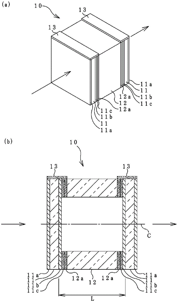
[0033] Such as figure 1 (a) and figure 1 As shown in (b), the etalon 10 according to Embodiment 1 of the present invention is mainly composed of two pairs of transparent members 11 , piezoelectric members 12 , and external connection terminals 13 .
[0034] The transparent members 11 are colorless and transparent materials such as glass and crystal, for example, and are used in pairs of two. These transparent members 11 are formed as parallel flat plates of a predetermined thickness, for example, as a quadrangle when viewed from above. Between the opposite main faces of these two transparent members is the resonator length L (refer to figure 1 (b)). The antireflection film 11a is provided on one main surface of these transparent members 11, and the reflection film 11b is provided on the other main surface. In addition, when referring to the main surface, the light incident / exiting surface is used as the main surface, and the four surfaces surrounding the main surface are u...
Embodiment approach 2
[0073] Such as Figure 5 As shown, the etalon device 101 according to Embodiment 2 of the present invention uses the etalon 10 according to Embodiment 1 of the present invention, and is mainly configured to include a variable voltage power supply 20 that 20 is connected to the external connection terminal 13 provided on the outer peripheral surface of the transparent member 11 which is one of the constituent elements of the etalon.
[0074] The voltage variable power supply 20 is, for example, a conventionally known variable voltage power supply, including wiring with + (positive) polarity and wiring with - (negative) polarity, so that the wiring with + polarity is connected to the outer periphery of the etalon 10 One external connection terminal 13 exposed on the etalon 10 is connected to the other external connection terminal 13 exposed on the outer peripheral surface of the etalon 10 to connect the -polarity wiring.
[0075] For example, for the case of the etalon involved...
Embodiment approach 3
[0081] Such as Figure 6 and Figure 7 As shown, the etalon device 102 according to Embodiment 3 of the present invention differs from Embodiment 2 in that a switch 30 for switching polarity is provided between the etalon 10 according to Embodiment 1 and the variable voltage power supply 20 .
[0082] The switch 30 functions to switch the polarity between the external connection terminal 13 provided on the etalon 10 and the variable voltage power supply 20 .
[0083] For example, the switch 30 includes a switching mechanism with a rotary structure, the terminal of the + polarity wiring connected to the variable voltage power supply 20 is set as A1, the terminal of the - polarity wiring is set as A2, and an external connection with the etalon 10 The terminals of the wiring connected to the terminal 13 are B1 and B2, and the terminals of the wiring connected to the other external connection terminal 13 of the etalon 10 are C1 and C2.
[0084] Here, each terminal is located on...
PUM
 Abstract
Description
Claims
Application Information


