Mixed wafer level vacuum packaging method and structure based on banding getter

A technology of vacuum encapsulation and getter, which is applied in the directions of microstructure devices without moving elements, microstructure technology, microstructure devices, etc., which can solve the problems of low efficiency, waste of infrared filters, poor performance, etc.

Active Publication Date: 2014-09-03
SHANGHAI INST OF MICROSYSTEM & INFORMATION TECH CHINESE ACAD OF SCI
View PDF4 Cites 17 Cited by
  • Summary
  • Abstract
  • Description
  • Claims
  • Application Information

AI Technical Summary

Problems solved by technology

The traditional vacuum packaging method is to use metal shells for packaging, generally including metal sockets and infrared filters. This vacuum packaging method is slightly less efficient; wafer-level vacuum packaging is to complete the vacuum packaging of the entire wafer before slicing. , improving the packaging efficiency, but due to the yield of the chips to be packaged, some chips with poor performance were packaged, wasting some expensive infrared filters

Method used


Image

  • Mixed wafer level vacuum packaging method and structure based on banding getter
  • Mixed wafer level vacuum packaging method and structure based on banding getter
  • Mixed wafer level vacuum packaging method and structure based on banding getter

Examples


Embodiment 1

[0089] This embodiment provides a hybrid wafer-level vacuum packaging method based on a strip-shaped getter, including the following steps:

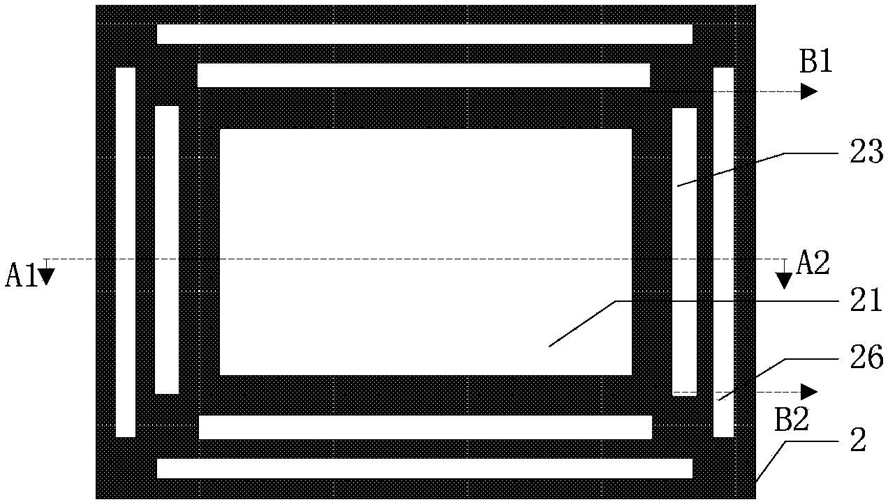
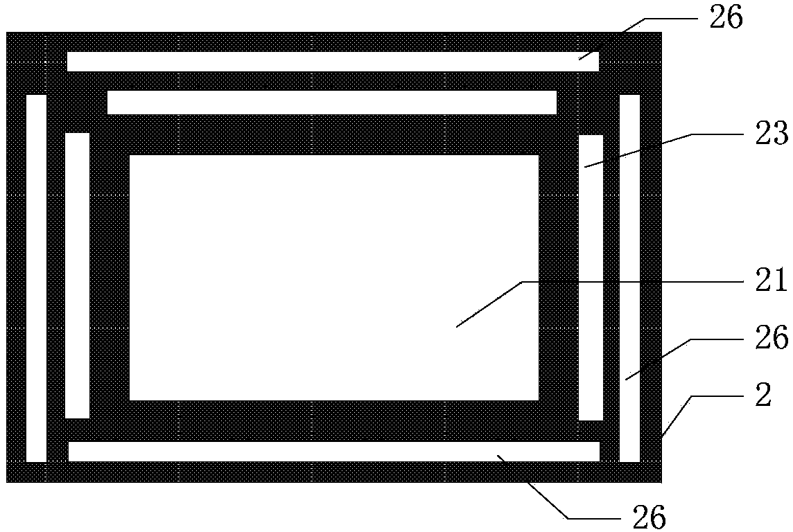
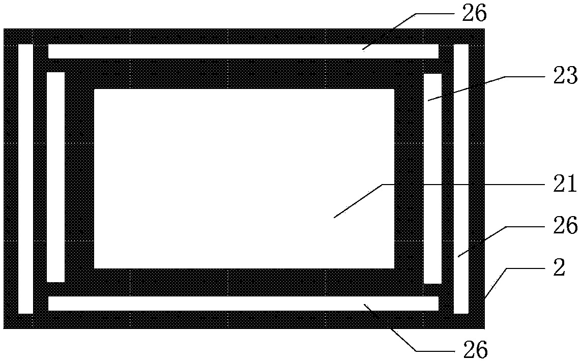
[0090] First carry out step a), provide a gasket 2, a substrate sheet 1 and a cover sheet, form a chip package cavity 21 and at least one getter cavity 23 in the gasket 2, and form a chip package cavity 21 in the chip package cavity 21 Vent holes 27 are formed in the spacer 2 between the getter chamber 23 and the getter chamber 23 .

[0091] Then proceed to step b), bonding the gasket 2 and the substrate 1 to form a package cavity.

[0092] Then proceed to step c), making composite metal layers 12, 22 on the upper surface of the substrate 1 and the gasket 2, or making a composite metal layer 22 on the upper surface of the gasket 2 and making a composite metal layer on the lower surface of the cover sheet.

[0093] Then proceed to step d), providing a chip to be packaged, bonding the chip to be packaged that has passed the test to the su...

Embodiment 2

[0132] Such as Figure 5 As shown, this embodiment provides a hybrid wafer-level vacuum packaging method based on a tape-shaped getter, and its basic steps are as in Embodiment 1, wherein the cover sheet is fixed on a surface that matches the size of the substrate sheet Separators in the jig.

[0133] Such as Figure 5 As shown, this embodiment also provides a hybrid wafer-level vacuum packaging structure based on a strip-shaped getter, the basic structure of which is as in Embodiment 1, wherein the cover sheet is fixed on a Separators in matching jigs.

Embodiment 3

[0135] Such as Figure 6 As shown, this embodiment provides a hybrid wafer-level vacuum packaging method based on a strip-shaped getter, and its basic steps are as in Embodiment 1, wherein, this embodiment does not need to form through holes in the substrate sheet and the chip to be packaged structure and metal posts, but form a through-hole structure for the leads of the chip to be packaged in the cover sheet, and form a metal post 33 in the through-hole structure of the cover sheet; the thermal infrared detector is not a bond bonded to the surface of the substrate but to the surface of the cover slip.

[0136] Such as Figure 6 As shown, this embodiment also provides a hybrid wafer-level vacuum packaging structure based on a strip-shaped getter. Hole structure and metal column, and the through-hole structure and metal column 33 used for the lead of the chip to be packaged are formed in the cover sheet; the thermal infrared detector is not bonded to the surface of the subst...


PUM


Abstract

The invention provides a mixed wafer level vacuum packaging method and structure based on a banding getter. The method includes the steps that (a) a gasket, a substrate slice and a cover slice are provided, a chip packaging cavity and a getter cavity are formed in the gasket, and air holes are further formed; (b) the gasket and the substrate slice are bonded to form a packaging cavity; (c) a chip to be packaged is provided, and the chip is bonded on the substrate slice through a bonding structure; (d) the getter is provided and fixed in the getter cavity; (e) the getter is activated, and the cover slice and the gasket are bonded. According to the mixed wafer level vacuum packaging method and structure based on the banding getter, the packaging cavity is made on the basis of an MEMS technology, the chip to be packaged is placed in the chip packaging cavity to complete vacuum packaging, a weak micro-structure on the chip to be packaged can be better protected, and the wafer level packaging efficiency is achieved; the getter cavity specially used for storing the banding getter is designed, and compared with a getter thin film and the like, cost is low; vacuum packaging is only conducted on the chip which already passes a test, and the packaging cost is lowered.

Description

technical field [0001] The invention relates to a hybrid wafer-level vacuum packaging method and structure, in particular to a hybrid wafer-level vacuum packaging method and structure based on a strip-shaped getter. Background technique [0002] Infrared detection technology is one of the modern core military technologies, which has the advantages of long detection distance, strong anti-interference ability, and can work around the clock. With the development and maturity of infrared imaging technology, its application in civilian fields is becoming more and more extensive. [0003] According to the working principle, infrared detectors can be divided into two categories: quantum type and thermal type. Quantum-type infrared detectors have high sensitivity, generally require refrigeration, and are expensive. Thermal infrared detectors are slightly less sensitive, do not require refrigeration, and are more cost-effective. This kind of uncooled infrared detector can be divid...

Claims


Application Information

Patent Timeline
Patent Type & Authority Applications(China)
IPC IPC(8): H01L21/50H01L23/16B81C3/00B81B7/02
CPCB81B1/002B81C1/00047H01L21/50H01L23/16H01L2224/16225
Inventor 冯飞张云胜王跃林
Owner SHANGHAI INST OF MICROSYSTEM & INFORMATION TECH CHINESE ACAD OF SCI
Why Eureka
Try Eureka