A chip-to-chip interconnection device based on fpga

A chip-to-chip technology, which is applied in the field of FPGA-based chip-to-chip interconnection devices, can solve problems that do not involve LVDS interfaces, and achieve the effect of adjustable speed and high flexibility

Active Publication Date: 2017-01-25
SHANDONG CHAOYUE DATA CONTROL ELECTRONICS CO LTD
View PDF3 Cites 0 Cited by
  • Summary
  • Abstract
  • Description
  • Claims
  • Application Information

AI Technical Summary

Problems solved by technology

[0003] There are many available technologies for the interconnection between chips. The LVDS (Low-Voltage Differential Signaling) interface has the characteristics of low noise, low power consumption, high speed, and low cost. When the speed requirement is not too high (usually These chips do not integrate serdes (serializer), and are often used as the interconnection interface between chips. In the existing technology, there is generally no LVDS interface with reliable data transmission and adjustable transmission rate.

Method used


Image

  • A chip-to-chip interconnection device based on fpga

Examples


Embodiment 1

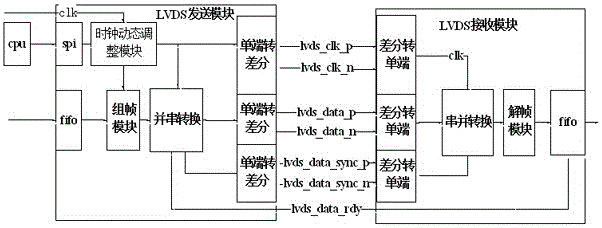
[0028] As attached figure 1 As shown, an FPGA-based inter-chip interconnection device is provided with a clock dynamic adjustment module, an LVDS sending module, and an LVDS receiving module in the FPGA chip.

[0029] Clock dynamic adjustment module:

[0030] In order to realize the dynamic reconfiguration of the rate, the scheme of dynamically reconfigurable clock is adopted, and the reconfigured clock parameters are sent to the clock dynamic adjustment module in the FPGA in real time through the spi or iic interface connected to the CPU and the FPGA. The clock output by the adjustment module is the clock of the entire device.

[0031] LVDS sending module:

[0032] The opposite end chip will send a data ready signal. When the opposite end module is ready to receive data, fifo will read the data in fifo every data bit width cycle. The read data will go through the framing module and follow the packet header. , Data length, valid data and data checksum protocol format framing at the ...


PUM


Abstract

The invention relates to the technical field of chip interconnection, in particular to an FPGA-based interconnection device among chips. According to the FPGA-based interconnection device among the chips, a dynamic clock adjusting module, a low-voltage differential signal sending module and a low-voltage differential signal receiving module are arranged in each FPGA chip so that information transmission between the FPGA chips can be achieved. The interconnection device has the advantages of being adjustable in speed and high in flexibility.

Description

Technical field [0001] The invention relates to the technical field of chip interconnection, in particular to an FPGA-based inter-chip interconnection device. Background technique [0002] FPGA (Field Programmable Gate Array) chip is a programmable logic device with short development cycle and high reliability. [0003] There are many available technologies for the interconnection between chips. LVDS (Low-Voltage Differential Signaling) interface has the characteristics of low noise, low power consumption, high speed, and low cost. When the speed requirement is not too high (usually These chips do not integrate serdes (serializers), and are often used as interconnect interfaces between chips. In the existing technology, there is generally no LVDS interface with reliable data transmission and adjustable transmission rate. Summary of the invention [0004] In order to solve the problems of the prior art, the present invention provides an FPGA-based inter-chip interconnection device, ...

Claims


Application Information

Patent Timeline
Patent Type & Authority Patents(China)
IPC IPC(8): G06F13/38
Inventor 秦刚刘强孙大军李长志
Owner SHANDONG CHAOYUE DATA CONTROL ELECTRONICS CO LTD
Why Eureka
Try Eureka