
Pixel Compensating Circuit

A compensation circuit and pixel technology, applied in the field of pixel compensation circuits, can solve the problems of insufficient compensation time, the panel cannot display gray scales correctly, and the display quality is reduced, so as to improve the accuracy, reduce the number of signal lines, and improve the luminous efficiency. Effect

Active Publication Date: 2014-09-10
AU OPTRONICS CORP
View PDF5 Cites 11 Cited by
  • Summary
  • Abstract
  • Description
  • Claims
  • Application Information

AI Technical Summary

Problems solved by technology

[0003] However, since the current value flowing through the organic light-emitting diode is affected by the driving transistor, the current value is related to the threshold voltage of the driving transistor, which will also reduce its display quality.
[0004] With the research and innovation of display technology and the needs of users, the requirements for panel resolution are also increasing. When the panel resolution becomes higher, the pixel compensation time will be reduced. However, the existing OLED pixel compensation circuit needs to be integrated in one The compensation of the line time is completed, and the compensation time of the current value flowing through the OLED is insufficient, so that the panel cannot correctly display its gray scale and reduce the display quality

Method used


Image

  • Pixel Compensating Circuit
  • Pixel Compensating Circuit
  • Pixel Compensating Circuit

Examples


Embodiment Construction

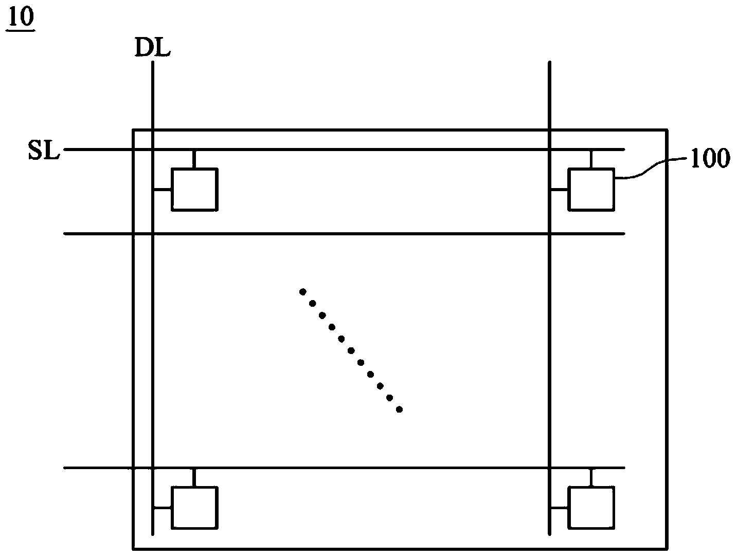
[0043] Please refer to figure 1 , figure 1 It is a schematic diagram of a display panel 10 according to an embodiment of the present invention. The display panel 10 includes a plurality of pixel compensation circuits 100, a plurality of data lines DL, and a plurality of scan lines SL, and each pixel compensation circuit 100 is connected to a corresponding data line DL and a scan line SL for receiving corresponding data signals and scan signal.

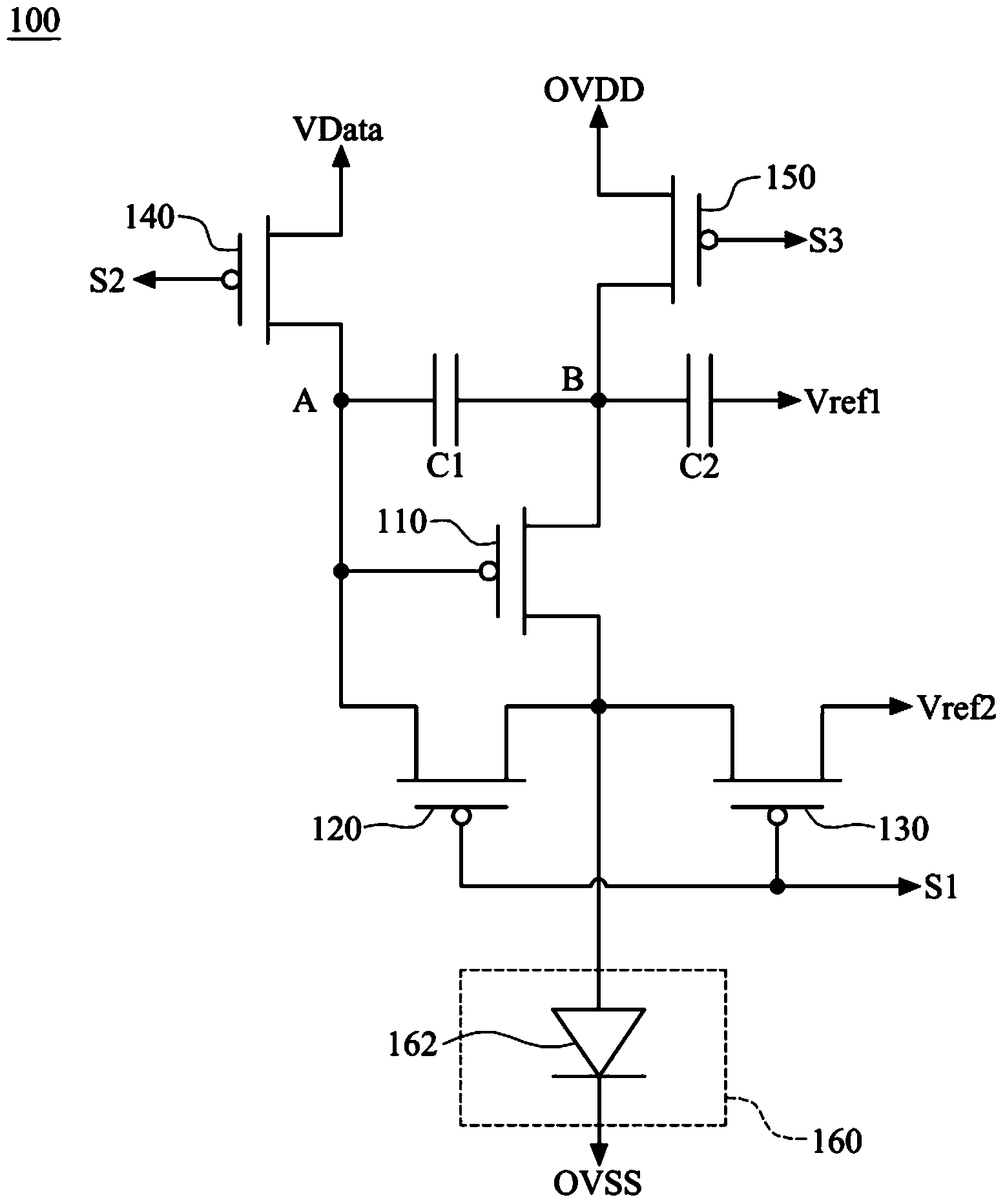
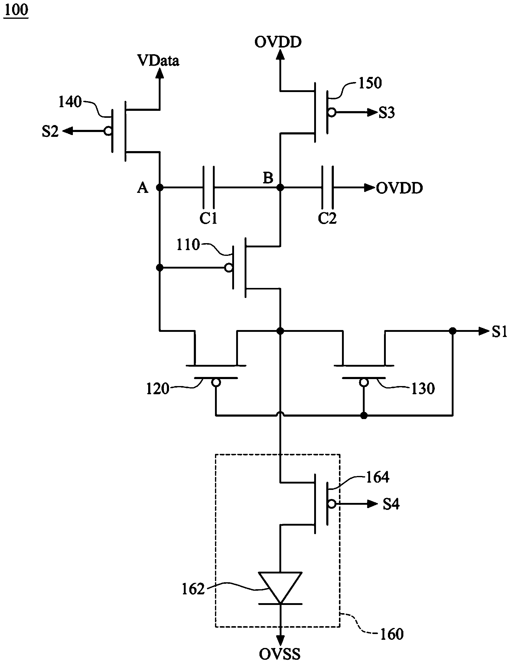
[0044] Please refer to figure 2 , figure 2 It is a schematic diagram of a pixel compensation circuit 100 according to an embodiment of the present invention, and a single pixel compensation circuit 100 will be described below. The pixel compensation circuit 100 includes a switch 110, a switch 120, a switch 130, a switch 140, a switch 150, a capacitor C1, a capacitor C2, and a light emitting unit 160. The switches respectively have a first end, a second end, and a control end; the capacitors respectively have a first end, a second...


PUM


Abstract

A pixel compensating circuit comprises a firs switch, a second switch, a third switch, a fourth switch, a fifth switch, a first capacitor, a second capacitor, and a luminescence unit. The first terminal of the second switch and the second terminal of the fourth switch are electrically connected to the control terminal of the first switch. The second terminal of the second switch and the first terminal of the third switch are electrically connected to the second terminal of the first switch. The control terminal of the third switch is electrically connected to the control terminal of the second switch and is used for receiving first scanning signal. The first terminal of the fourth switch is used for receiving data signal. The control terminal of the fourth switch is used for receiving second scanning signal. The first terminal of the fifth switch is electrically connected to a first voltage source, the second terminal of the fifth switch is electrically connected to the first terminal of the first switch, and the control terminal of the fifth switch is used for receiving third scanning signal. The first capacitor is electrically connected between the first terminal of the first switch and the control terminal of the first switch. The second capacitor is electrically connected to the first terminal of the first switch. The luminescence unit is coupled between the first switch and a second voltage source.

Description

technical field [0001] The invention relates to a pixel compensation circuit, in particular to a pixel compensation circuit of an organic light emitting diode. Background technique [0002] An organic light-emitting diode display panel (Organic Light-Emitting Display; OLED) is a display panel currently being developed and used, which has the advantages of thinness, lightness, power saving, and saturated chroma. [0003] However, since the current value flowing through the organic light emitting diode is affected by the driving transistor, the current value is related to the threshold voltage of the driving transistor, which also reduces the display quality. [0004] With the research and innovation of display technology and the needs of users, the requirements for panel resolution are also increasing. When the panel resolution becomes higher, the pixel compensation time will be reduced. However, the existing OLED pixel compensation circuit needs to be integrated in one Afte...

Claims


Application Information

Patent Timeline
IPC IPC(8): G09G3/32G09G3/3208
CPCG09G2300/0819
Inventor 蔡永胜林钰凯叶佳元刘俊彥
Owner AU OPTRONICS CORP
Features
  • Generate Ideas
  • Intellectual Property
  • Life Sciences
  • Materials
  • Tech Scout
  • Unparalleled Data Quality
  • Higher Quality Content
  • 60% Fewer Hallucinations
Learn More