Pixel structure and manufacturing method thereof
A pixel structure, pixel electrode technology, applied in nonlinear optics, instruments, optics, etc., can solve problems such as sacrificing aperture ratio, and achieve the effect of improving aperture ratio
- Summary
- Abstract
- Description
- Claims
- Application Information
AI Technical Summary
Problems solved by technology
Method used
Image

Examples
Embodiment 1
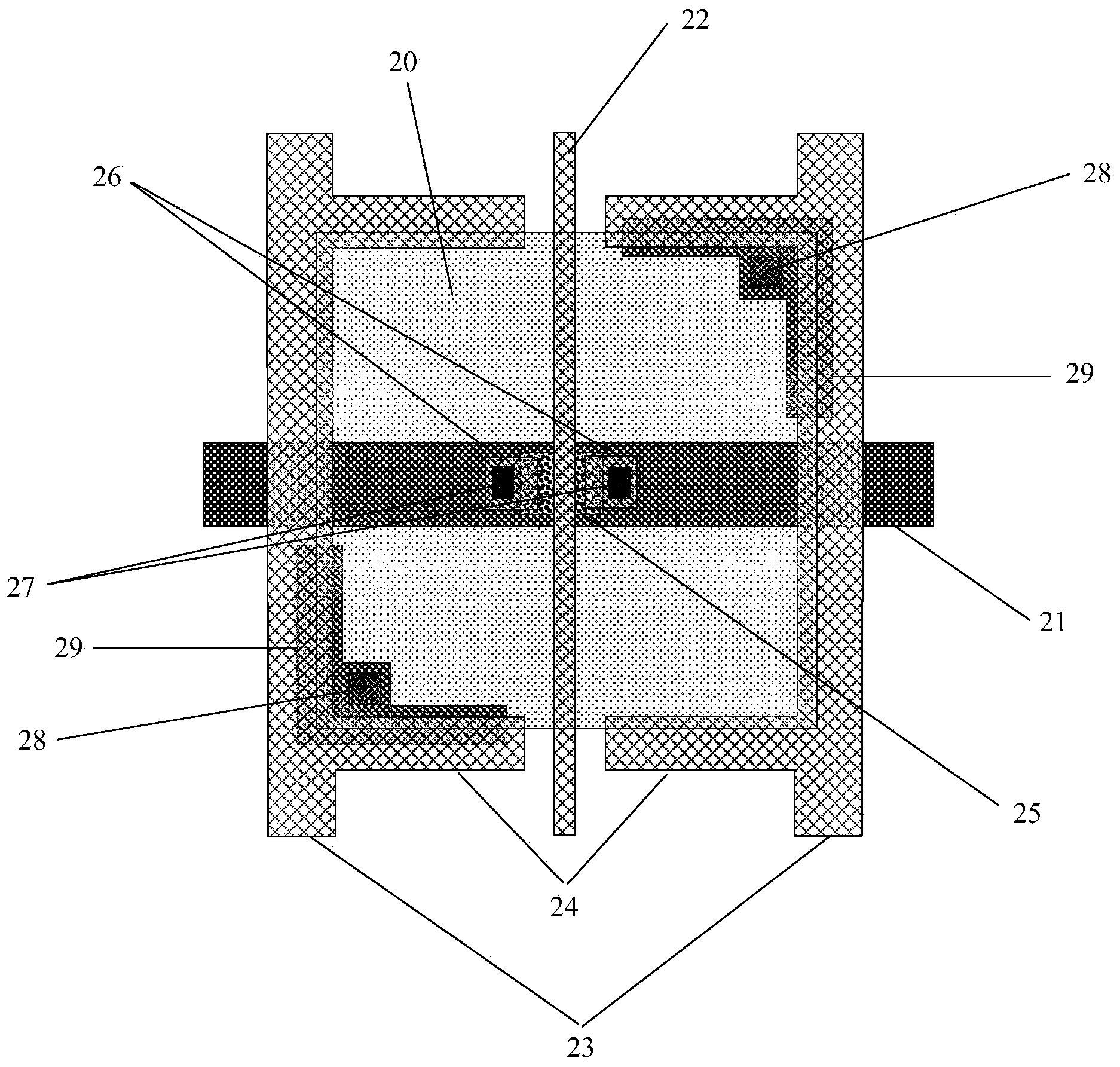
[0046] figure 2 It is a pixel structure of the first embodiment of the present invention. Such as figure 2 As shown, the present invention provides a substrate (not shown), which is provided with: a first common electrode line 24, a non-continuous distribution line with a gap; a second common electrode line 23, and the first common electrode line 24 Intersect to enclose the pixel area; a data line 22 is arranged on the vertical center line of the pixel area and passes through the gap of the first common electrode line 24; a scanning line 21 is arranged on the horizontal center line of the pixel area , and intersect with the data line 22; an active element, disposed at the intersection area of the data line 22 and the scan line 21; a pixel electrode 20, electrically connected to the active element through two first contact holes 27; The storage electrode 29 is disposed below the pixel electrode 20 and overlaps with the projections of the first common electrode 24 and the ...
Embodiment 2
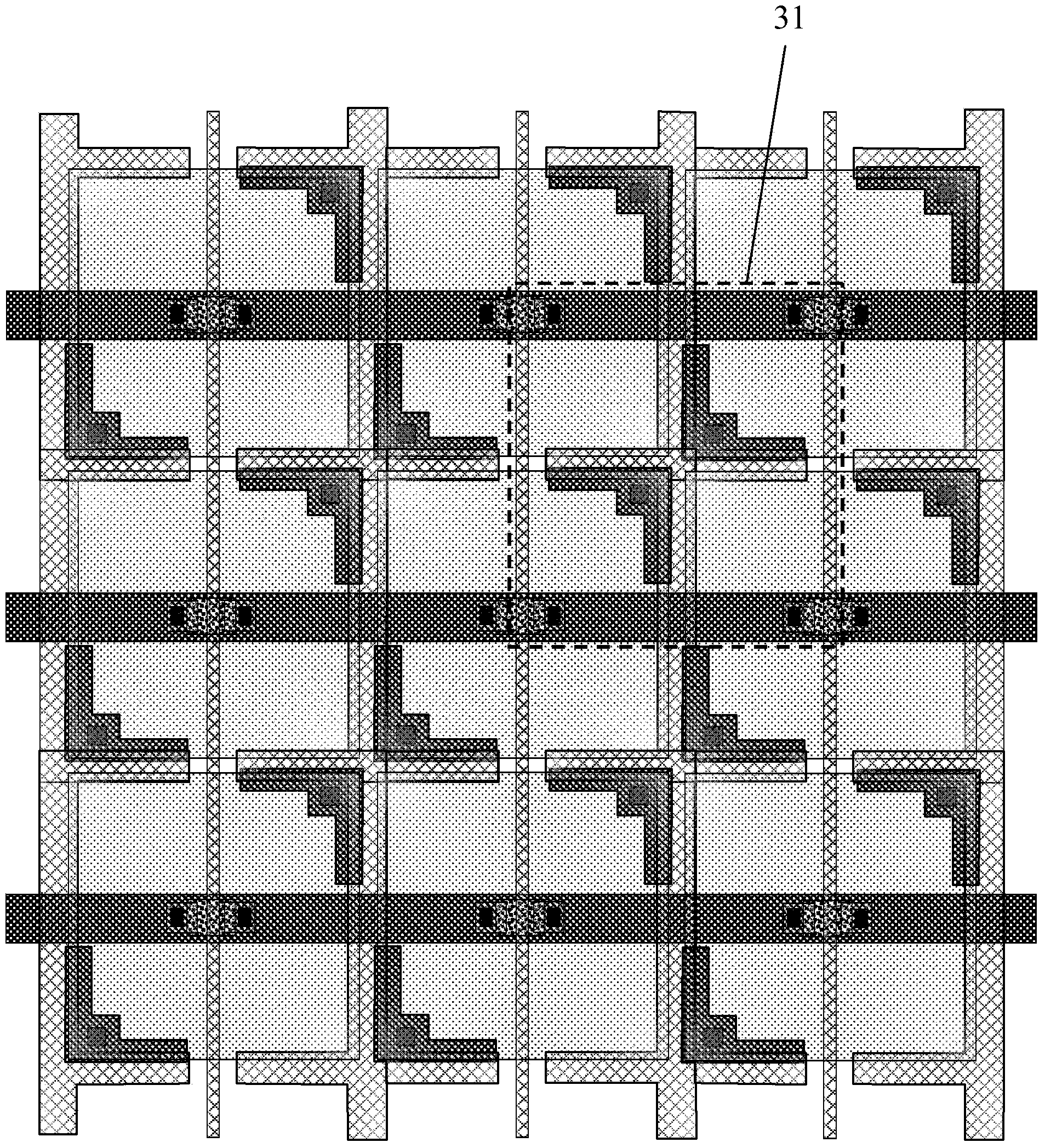
[0064] Figure 10 It is a schematic diagram of a pixel structure according to the second embodiment of the present invention. Such as Figure 10 As shown, the difference between the pixel structure and its manufacturing method provided by this embodiment and the first embodiment is that the storage electrode is arranged at the upper left corner and the lower right corner of the pixel area, and overlaps with the common electrode line to form a storage capacitor.
[0065] Through the pixel structure provided by this embodiment, the aperture ratio of the pixel can also be greatly increased; at the same time, the storage capacitor formed by overlapping the storage electrode and the common electrode line can also automatically compensate the size of the storage capacitor when the upper and lower metal layers are shifted.
Embodiment 3
[0067] Figure 11 It is a schematic diagram of a pixel structure according to the third embodiment of the present invention. Such as Figure 11 As shown, the difference between the pixel structure and its manufacturing method provided by this embodiment and the first embodiment is that, except for the area where the contact hole is arranged, the storage electrode completely overlaps with the projected area of the first and second common electrode lines to form a storage capacitor .
[0068] Through the pixel structure provided by this embodiment, the aperture ratio of the pixel can also be greatly increased; at the same time, the storage capacitor formed by overlapping the storage electrode and the common electrode line can also automatically compensate the size of the storage capacitor when the upper and lower metal layers are shifted.
PUM
| Property | Measurement | Unit |
|---|---|---|
| Thickness | aaaaa | aaaaa |
Abstract
Description
Claims
Application Information
 - Generate Ideas
- Intellectual Property
- Life Sciences
- Materials
- Tech Scout
- Unparalleled Data Quality
- Higher Quality Content
- 60% Fewer Hallucinations
Browse by: Latest US Patents, China's latest patents, Technical Efficacy Thesaurus, Application Domain, Technology Topic, Popular Technical Reports.
© 2025 PatSnap. All rights reserved.Legal|Privacy policy|Modern Slavery Act Transparency Statement|Sitemap|About US| Contact US: help@patsnap.com