Output drive device and output drive method

An output drive technology, applied in the field of output drive devices, can solve problems such as transistor breakdown, achieve the effect of suppressing current spikes and avoiding junction breakdown

Active Publication Date: 2016-08-17
NXP BV
View PDF5 Cites 0 Cited by
  • Summary
  • Abstract
  • Description
  • Claims
  • Application Information

AI Technical Summary

Problems solved by technology

For example, if the transistor's junction breakdown voltage is less than the maximum supply voltage for the load, the transistor may break down due to overstress

Method used


Image

  • Output drive device and output drive method
  • Output drive device and output drive method
  • Output drive device and output drive method

Examples


Embodiment Construction

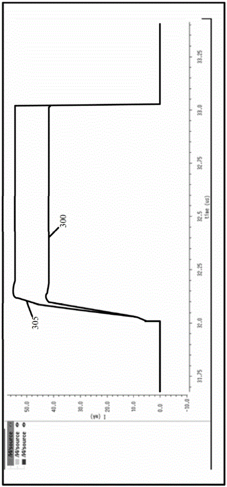
[0020] Aspects of the present invention may be employed in many different types of devices, systems and structures for controlling current flow through a load located in a controlled current path based on a modulated voltage signal. For a load, such as a light-emitting diode (LED) strip, controlling its current can prevent a peak current from flowing into the LED strip when the LED is turned on or off. Spike currents can cause unwanted brightness and flickering effects on LEDs. Aspects of the invention can be demonstrated by the various examples described above and below, the invention is not limited to the examples described.

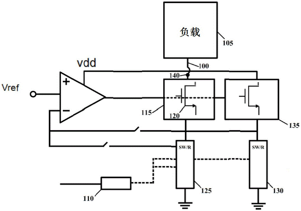
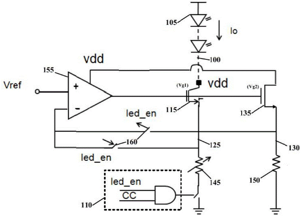
[0021] Exemplary embodiments of the present invention provide methods and apparatus that include a controlled current path that includes a load (such as an LED strip) that draws current from the controlled current path. Responsive to the first aspect and the second aspect of the modulated voltage signal, a control circuit is provided to control the fl...


PUM


Abstract

The invention relates to an output driving device and an output driving method. Exemplary embodiments of the present invention include a controlled current path having a load that draws current from the controlled current path. In response to the modulated voltage signal, current flow through the load of the controlled current path is controlled by causing a transistor circuit including a transistor to switch between two modes. This switching subjects the junction of the transistor to a voltage stress caused by the current spike in the controlled current path towards the breakdown threshold of the transistor. Current in the controlled current path is directed through the first current branch in response to the first aspect of the modulated voltage signal and in one of the current modes. Current in the controlled current path is diverted from the first current branch to the second current branch in response to the second aspect of the modulated voltage signal and in another current mode.

Description

technical field [0001] The invention relates to an output driving device and an output driving method. Background technique [0002] Voltage-to-current (V2I) converters are useful as output drivers to control the current flowing through a load, such as a light-emitting diode (LED) strip. Specifically, a current mode controller (with low-side control) can control the current through the LED through a connection to the drain of the NMOS transistor. The reason for using this type of setup is that NMOS transistors can withstand high voltages, such as extended drain NMOS (EDNMOS), for many LEDs. [0003] An example of an arrangement for a V2I converter is to use a reference voltage applied to the non-inverting node of the feedback amplifier. The amplifier has a high open-loop gain, which ensures that the source voltage is equal to the reference voltage. An NMOS transistor (N-type MOSFET) connected to the output of the amplifier acts as a source follower. The negative feedback...

Claims


Application Information

Patent Timeline
Patent Type & Authority Patents(China)
IPC IPC(8): H05B37/02H05B44/00
CPCH05B45/327H05B45/397Y02B20/30H05B45/54
Inventor 阿布·卡迈勒詹姆士·卡拉维拉
Owner NXP BV
Why Eureka
Try Eureka