Liquid crystal panel and display device
A technology for liquid crystal panels and array substrates, applied in the field of liquid crystal panels and display devices, capable of solving problems such as voltage instability and affecting the display effect of liquid crystal displays, achieving stable voltage and improving display effects
- Summary
- Abstract
- Description
- Claims
- Application Information
AI Technical Summary
Problems solved by technology
Method used
Image

Examples
Embodiment 1
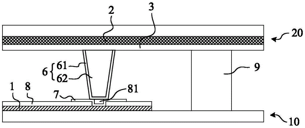
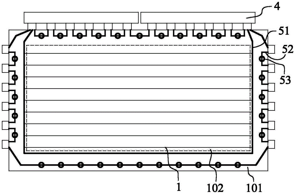
[0033] Such as figure 1 and figure 2 As shown, the liquid crystal panel provided by the embodiment of the present invention includes an array substrate 10 and a color filter substrate 20 . Components such as common electrode lines 1 are disposed on the array substrate 10 , and components such as a color filter layer (not shown in the figure), black matrix 2 , and common electrodes 3 are disposed on the color filter substrate 20 . Both the common electrode line 1 and the common electrode 2 are supplied with voltage by a power supply circuit (not shown in the figure) in the circuit board 4 , and the power supply circuit provides equal voltages to the common electrode line 1 and the common electrode 3 .
[0034] The power supply circuit is connected to the common electrode line 1 through the first wiring 51 on the array substrate 10 . On the other hand, the power supply circuit is connected to the common electrode 3 on the color filter substrate 20 through the second wiring 52...
Embodiment 2
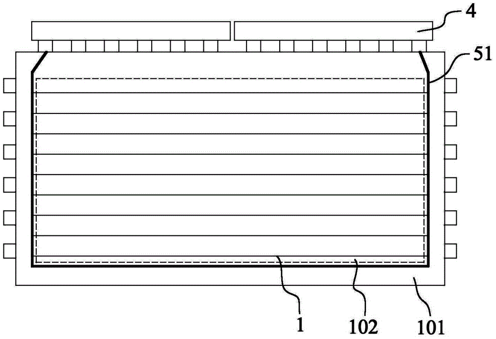
[0047] This embodiment is basically the same as Embodiment 1, the difference is that, as image 3 As shown, the second wiring and the conductive gold ball in the first embodiment are omitted in this embodiment.
[0048] Because the power supply circuit in the circuit board 4 provides the same voltage for the common electrode line 1 and the common electrode 3, so in this embodiment, the power supply circuit provides voltage for the common electrode line 1 on the array substrate 10 through the first wiring 51 , and then provide voltage to the common electrode 3 on the color filter substrate 20 through the common electrode line 1 and the conductive connector. Therefore, the second wiring and the conductive gold ball in Embodiment 1 can be omitted without affecting the stability of the voltage on the common electrode 3, thereby reducing the wiring in the edge area 101 of the array substrate 10 and making the liquid crystal panel It can have a narrower frame, and the LCD panel can...
Embodiment 3
[0050] An embodiment of the present invention provides a display device, which may be a liquid crystal television, a liquid crystal display, a mobile phone, a tablet computer, and the like. The display device includes the liquid crystal panel provided in Embodiment 1 or Embodiment 2 above, and components such as a backlight module.
PUM
 Abstract
Description
Claims
Application Information
 - Generate Ideas
- Intellectual Property
- Life Sciences
- Materials
- Tech Scout
- Unparalleled Data Quality
- Higher Quality Content
- 60% Fewer Hallucinations
Browse by: Latest US Patents, China's latest patents, Technical Efficacy Thesaurus, Application Domain, Technology Topic, Popular Technical Reports.
© 2025 PatSnap. All rights reserved.Legal|Privacy policy|Modern Slavery Act Transparency Statement|Sitemap|About US| Contact US: help@patsnap.com