Fabrication method for organic EL device

An electroluminescence device and a manufacturing method technology, which are applied in the directions of organic semiconductor devices, semiconductor/solid-state device manufacturing, circuits, etc.

Inactive Publication Date: 2014-10-01
SEIKO EPSON CORP
View PDF1 Cites 16 Cited by
  • Summary
  • Abstract
  • Description
  • Claims
  • Application Information

AI Technical Summary

Problems solved by technology

[0004] However, in order to set the optimum optical path length, it is necessary to form the thickness of the laminated film such as a transparent conductive film in each light-emitting region corresponding to the required wavelength of each color, so the There is a difference in height around the pixel area, etc.
Therefore, there is a problem that when a level difference is formed around the pixel area, unintended parasitic light emission will occur due to a deviation in the value of the optimum optical path length (resonance). lights of different colors

Method used


Image

  • Fabrication method for organic EL device
  • Fabrication method for organic EL device
  • Fabrication method for organic EL device

Examples


Embodiment Construction

[0028] Hereinafter, preferred embodiments of the present invention will be described in detail using the drawings. In addition, the embodiment described below is not an aspect which unreasonably limits the content of this invention described in a claim. In addition, not all the configurations described below are necessarily essential components of the present invention.

[0029] 1. Structure of organic EL device

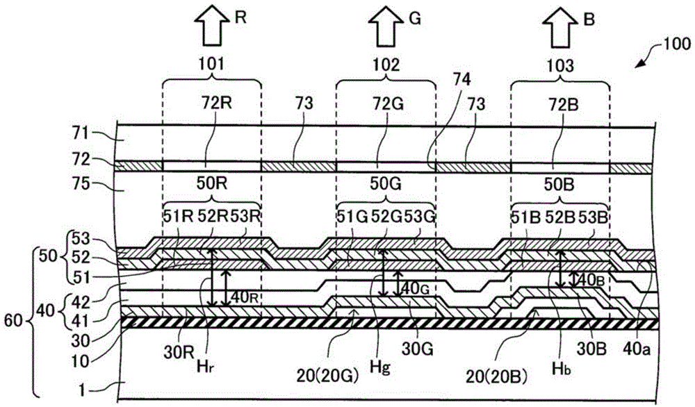
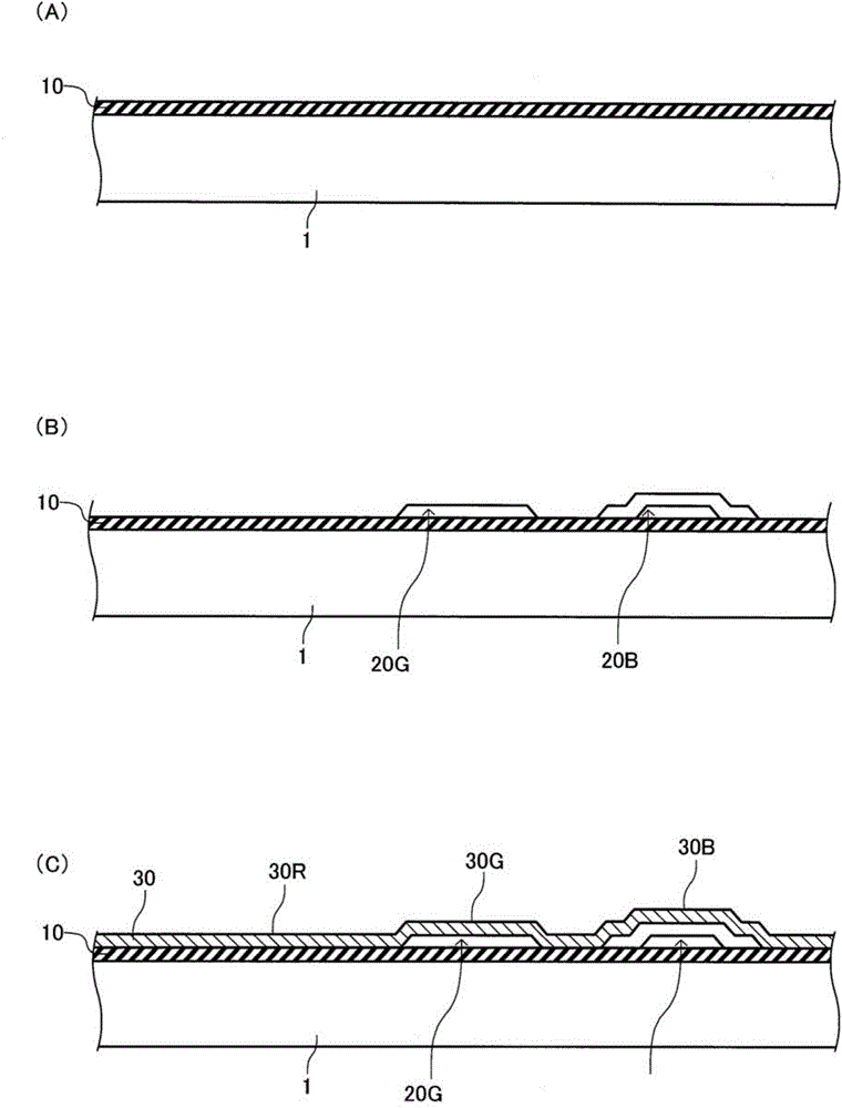
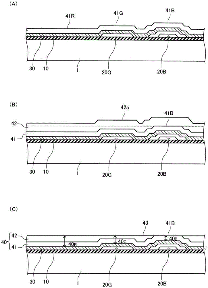
[0030] First, the organic EL device 100 manufactured by the method for manufacturing the organic EL device according to the present embodiment will be described with reference to the accompanying drawings. figure 1 It is a cross-sectional view schematically showing the organic EL device 100 . In addition, in order to express the structure in an easy-to-understand manner, the ratio of the layer thickness to the dimension, the angle, and the like of each component are appropriately different. exist figure 1 In , the white hollow arrow marks indicate the light emitt...


PUM


Abstract

The fabrication method for an organic EL device according to the invention includes: forming a third insulating layer on a first insulating layer; removing the third insulating layer in a first pixel region by etching the third insulating layer; forming a second insulating layer that has different thicknesses in a first pixel and a second pixel and has a flat first surface by forming a precursor insulating layer to continuously cover a first reflection film and a second reflection film and then planarizing an upper surface of the precursor insulating layer; and forming a first pixel electrode and a second pixel electrode on the first surface of the second insulating layer. The first insulating layer is slower in the rate at which the layer is removed by etching than the third insulating layer.

Description

technical field [0001] The invention relates to a manufacturing method of an organic electroluminescent device. Background technique [0002] An organic EL (electroluminescence) device has a structure in which a light-emitting layer made of a light-emitting material is sandwiched between an anode (pixel electrode) and a cathode (counter electrode). For example, as described in Patent Document 1, there is known a resonance structure in which a reflective film is provided on the opposite side of the light-emitting layer in the anode, and light emitted from the light-emitting layer is transmitted between the reflective film and the cathode. back and forth, thereby selecting light with a spectrum with a higher peak intensity and a narrower width. According to such a structure, the color reproducibility of light emission can be improved. [0003] As a method of manufacturing an organic EL device, for example, an anode is formed on a reflective film, and a transparent conductive...

Claims


Application Information

Patent Timeline
Patent Type & Authority Applications(China)
IPC IPC(8): H01L21/77H01L51/56
CPCH01L51/56H01L51/5262H01L2227/323H01L51/5036H01L27/3211H01L2251/5315H01L51/5218H01L2251/558H01L51/5256H10K50/852H10K71/00H10K50/85H10K50/125H10K50/818H10K50/856H10K50/8445H10K59/35H10K59/1201H10K2102/351H10K2102/3026
Inventor 佐藤久克村田贤志
Owner SEIKO EPSON CORP
Why Eureka
Try Eureka