Supercharge Your Innovation With Domain-Expert AI Agents!

System and method for inspecting wire bonding

A technology of leads and pins, which is applied in the field of inspection of lead welding systems, and can solve problems such as errors in inspection results, distinction between various components and leads, and image distortion

Inactive Publication Date: 2016-11-30
ISMEDIA
View PDF4 Cites 0 Cited by
  • Summary
  • Abstract
  • Description
  • Claims
  • Application Information

AI Technical Summary

Problems solved by technology

However, since there are various parts between the pads of the semiconductor chip and the lands on the substrate, it may be difficult to distinguish the various parts and leads on the captured image
In this case, since the precise connection status of the lead wires cannot be acquired, there may be an error in the inspection result
In addition, the image may be distorted depending on the illuminance of the lighting device and the lighting position, and an error may occur in the detection result depending on the skill of the inspection program operator or the work environment

Method used


Image

  • System and method for inspecting wire bonding
  • System and method for inspecting wire bonding
  • System and method for inspecting wire bonding

Examples


specific Embodiment approach

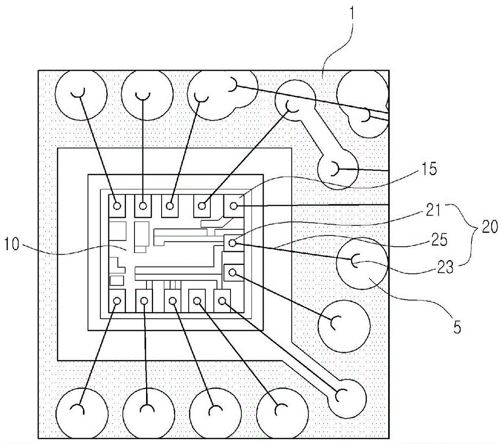
[0038] In the following, reference will be made to figure 2 Describes a method for checking such as figure 1 Shows whether the leads of the substrate on which the semiconductor chip is mounted are properly soldered or not.

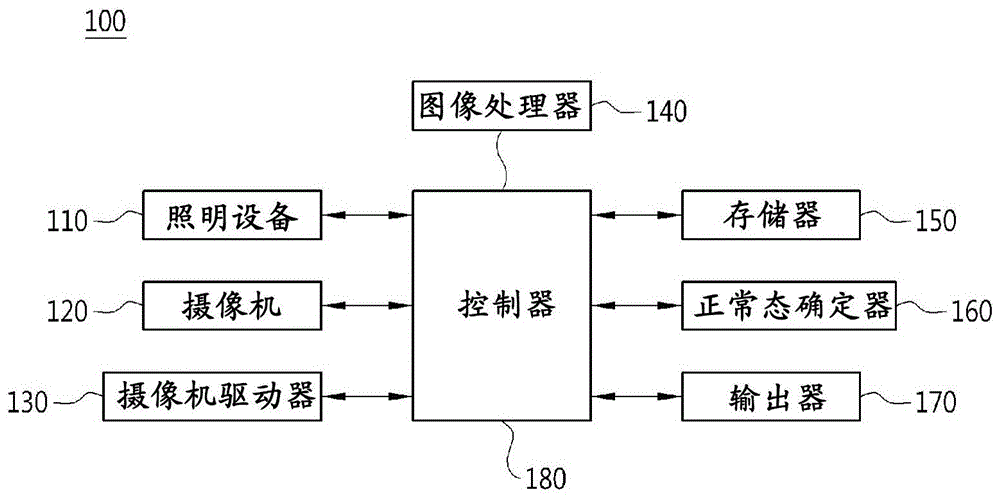
[0039] figure 2 is a block diagram illustrating the configuration of a wire bonding inspection system according to an exemplary embodiment of the present invention.

[0040] refer to figure 1 and figure 2 , the wire bonding inspection system 100 according to the present invention photographs the substrate 1 on which the chip 10 is bonded as a 2D image, and determines whether the wires 20 are normally connected. To achieve this, the wire bonding inspection system 100 may include an illumination device 110 , a camera 120 , a camera driver 130 , an image processor 140 , a memory 150 , a normal state determiner 160 , an outputter 170 and a controller 180 .

[0041] In order for the camera 120 to capture accurate images, the lighting device 110 emits li...


PUM


Abstract

A system and method for inspecting wire bonding is provided. The system includes: a camera for photographing a substrate on which a semiconductor chip is mounted; an image processor for detecting an inspection target lead part from an image of the substrate photographed by the camera; a memory for storing reference data, the reference data is a standard for determining whether the detected inspection target lead part is normally connected; and a normal state determiner for determining whether the lead is normally connected by using the angle of the inspection target lead part and the reference data. The system may further include: a camera driver for adjusting the height of the camera; and a controller for controlling the camera driver to take a plurality of images of the substrate while changing the height of the camera. Therefore, it is possible to determine whether the wire is normally bonded by using the wire bonding direction in the 2D image, and thus the accuracy of the wire bonding inspection can be improved and the processing thereof can be simplified.

Description

technical field [0001] The present invention relates to a system and method for inspecting wire bonding, and more particularly, to whether a wire is normally bonded can be determined by using a wire bonding direction in a 2-dimensional image, and thus the accuracy of wire bonding inspection can be improved and A system and method for inspecting wire bonding that simplifies its handling. Background technique [0002] In general, a substrate on which a semiconductor chip including pads formed on a wafer serving as input / output terminals is used in electronic components, and the thus manufactured semiconductor chip is mounted on the substrate. [0003] The process of mounting the semiconductor chip includes a process of individualizing the semiconductor chip, a process of bonding the individualized semiconductor chip to a substrate, a process of connecting the semiconductor chip and the substrate via conductive leads, and a process of molding the semiconductor chip. [0004] T...

Claims


Application Information

Patent Timeline
Patent Type & Authority Patents(China)
IPC IPC(8): H01L21/60
Inventor 金钟元杨尚奎
Owner ISMEDIA
Features
  • R&D
  • Intellectual Property
  • Life Sciences
  • Materials
  • Tech Scout
  • Unparalleled Data Quality
  • Higher Quality Content
  • 60% Fewer Hallucinations
Learn More