Preparation method of TEM plane sample

A planar sample and sample technology, applied in the field of TEM planar sample preparation, can solve problems such as analysis limitations and achieve the effect of making up for analysis limitations

Active Publication Date: 2014-11-19
SEMICON MFG INT (SHANGHAI) CORP
View PDF5 Cites 8 Cited by
  • Summary
  • Abstract
  • Description
  • Claims
  • Application Information

AI Technical Summary

Problems solved by technology

[0005] The purpose of the present invention is to provide a method for preparing a TEM planar...

Method used


Image

  • Preparation method of TEM plane sample
  • Preparation method of TEM plane sample
  • Preparation method of TEM plane sample

Examples


Embodiment Construction

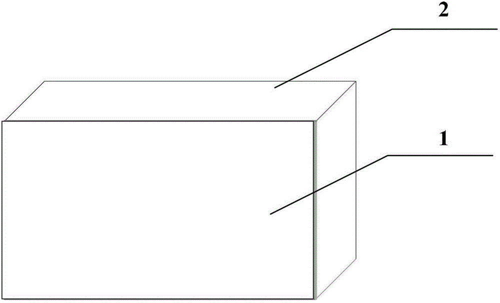
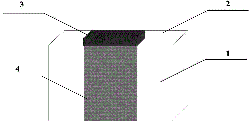
[0029] The preparation method of the TEM planar sample proposed by the present invention will be further described in detail below in conjunction with the accompanying drawings and specific examples. Advantages and features of the present invention will be apparent from the following description and claims. It should be noted that all the drawings are in a very simplified form and use imprecise scales, and are only used to facilitate and clearly assist the purpose of illustrating the embodiments of the present invention.

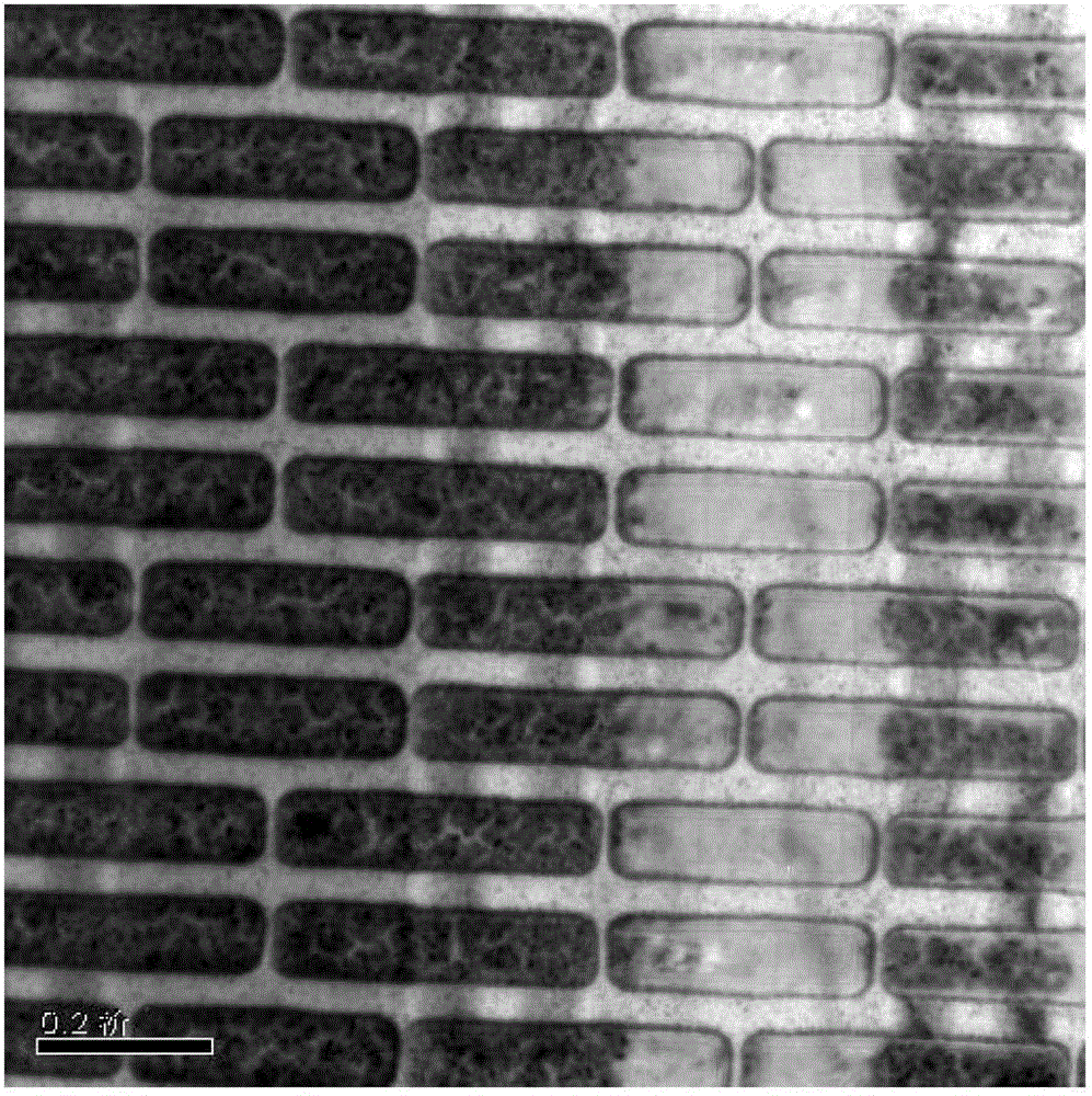
[0030] The TEM samples used in the existing TEM analysis are generally cross-sectional samples, and the filling ability of the thin film can be observed through the cross-section, but the cross-sectional samples have analysis limitations. In this regard, the inventors considered assisting the observation of cross-sectional samples by observing in the plane direction. Because the observation area of ​​the planar sample is larger than that of the cross-sectio...


PUM

PropertyMeasurementUnit
Thicknessaaaaaaaaaa

Abstract

The invention provides a preparation method of a TEM plane sample. The preparation method comprises the following steps: providing a wafer, wherein the wafer comprises a substrate and a semiconductor device layer; coating the semiconductor device layer with an organic matter film; cutting the wafer coated with the organic matter film to form a to-be-tested sample; forming a protection layer on the surface adjacent to the surface coated with the organic matter film; executing ionic thinning on the to-be-tested sample to form the TEM plane sample. In the preparation method of the TEM plane sample, provided by the invention, the organic matter film of a certain thickness covers the sample, thus a material of the protection layer is prevented from being splashed on the sample to influence the observation of the sample in a sample preparing process. Therefore, a clear TEM image of the plane sample can be obtained, thus the purpose of observing and analyzing the filling capability of the film by using the plane sample is realized, and the analysis limitation of a section sample in the prior art is made up.

Description

technical field [0001] The invention relates to the technical field of semiconductor detection, in particular to a method for preparing a TEM plane sample. Background technique [0002] With the development of semiconductor manufacturing process, the critical dimensions of semiconductor devices are getting smaller and smaller. The filling capability of the film has become a challenge for 45nm and more advanced processes. The improvement of the filling capacity of thin film also depends on the improvement of thin film analysis technology. In recent years, the rapid development of electron microanalysis technology has provided many analytical and testing methods for studying the microscopic state of thin film materials. Among them, the transmission electron microscope (TEM) is one of the most commonly used thin film analysis equipment. [0003] The working principle of a transmission electron microscope (TEM) is to make a TEM sample suitable for observation by cutting, grin...

Claims


Application Information

Patent Timeline
IPC IPC(8): G01N1/28
Inventor 赵燕丽齐瑞娟王小懿段淑卿
Owner SEMICON MFG INT (SHANGHAI) CORP
Why Eureka
Try Eureka