Analysis method for measuring large-grained silicon steel texture
An analytical method, a large-grain technology, applied in the analysis of materials, material analysis using wave/particle radiation, image analysis, etc., can solve problems such as inverse pole diagrams that cannot be used to draw large-grain silicon steel samples
- Summary
- Abstract
- Description
- Claims
- Application Information
AI Technical Summary
Problems solved by technology
Method used
Image
Examples
Embodiment Construction
[0013] The present invention will be described in further detail below in conjunction with the accompanying drawings and embodiments, but these embodiments should not be construed as limiting the present invention.
[0014] In a specific embodiment of the present invention: since the surface to be tested of the silicon steel plate must be a flat surface, it meets the requirements of the electron backscattered diffraction test after polishing and other pretreatments. Then cut a piece of large-grained silicon steel of 300mm×30mm to be the area to be tested for the electron backscattered diffraction sample.
[0015] like figure 1 As shown in , mark the grain boundaries with a marker pen to divide each grain; the marked grains are numbered from 1 to 48 in sequence.
[0016] Take this sample into a photo, and use an image analyzer to measure the area of each grain in the photo: A 1 to A 48 .
[0017] Calculate A 0 the size of:
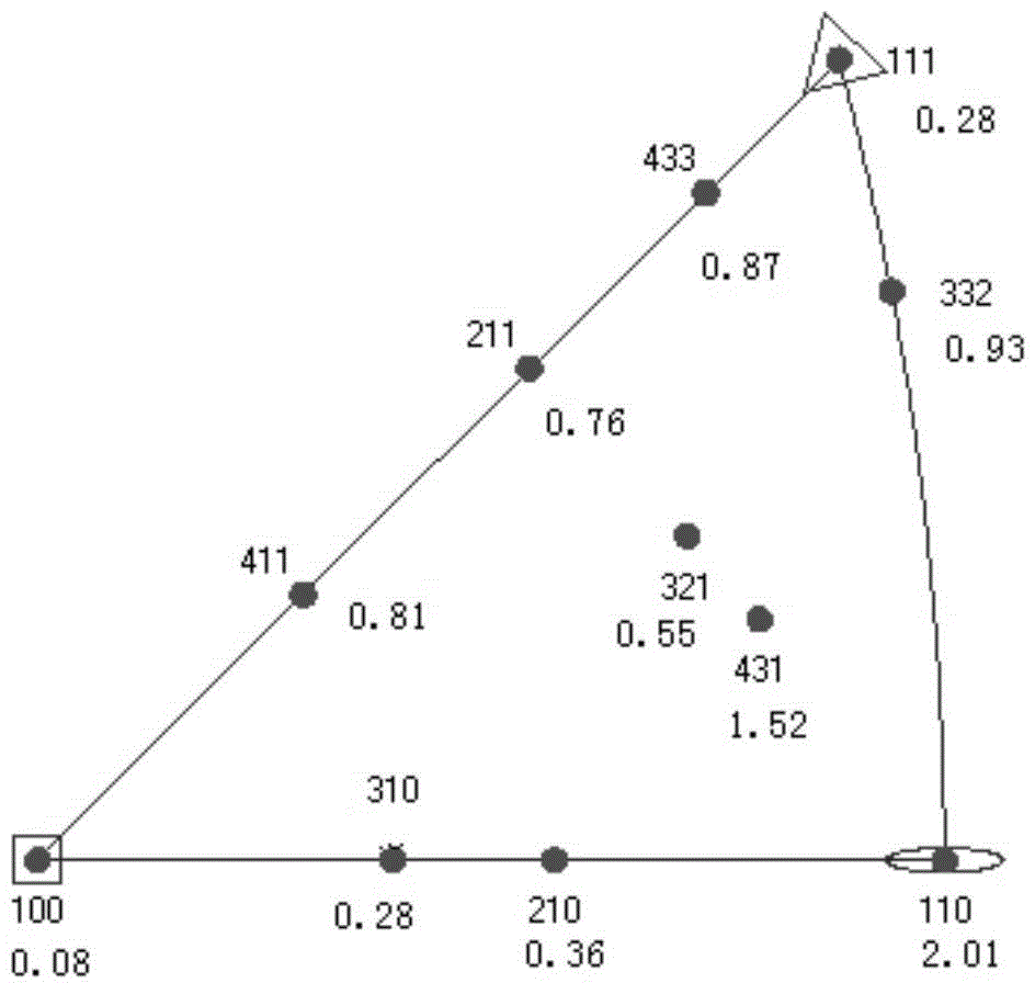
[0018] When surveying and mapping, the {hkl} ...
PUM
 Abstract
Description
Claims
Application Information

