OLED (Organic Light Emitting Diode) display device and manufacturing method thereof as well as display device

A technology for display devices and display devices, applied in semiconductor/solid-state device manufacturing, electric solid-state devices, semiconductor devices, etc., can solve the problems of large cathode transmission resistance, uneven brightness, large voltage drop, etc., and achieve long conduction time and high brightness Uniform, good electrical conductivity

Inactive Publication Date: 2014-11-19
BOE TECH GRP CO LTD
View PDF3 Cites 23 Cited by
  • Summary
  • Abstract
  • Description
  • Claims
  • Application Information

AI Technical Summary

Problems solved by technology

[0006] Embodiments of the present invention provide an OLED display device, a manufacturing method thereof, and a display device, which solve the

Method used


Image

  • OLED (Organic Light Emitting Diode) display device and manufacturing method thereof as well as display device
  • OLED (Organic Light Emitting Diode) display device and manufacturing method thereof as well as display device
  • OLED (Organic Light Emitting Diode) display device and manufacturing method thereof as well as display device

Examples


Embodiment Construction

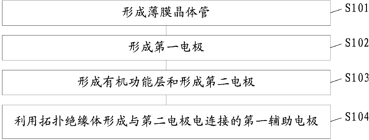
[0028] The following will clearly and completely describe the technical solutions in the embodiments of the present invention with reference to the accompanying drawings in the embodiments of the present invention. Obviously, the described embodiments are only some, not all, embodiments of the present invention. Based on the embodiments of the present invention, all other embodiments obtained by persons of ordinary skill in the art without making creative efforts belong to the protection scope of the present invention.

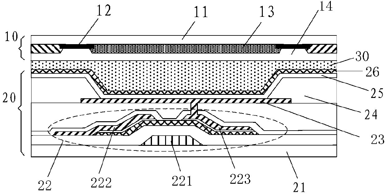
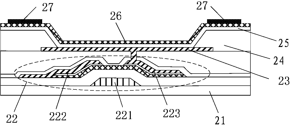
[0029] Topological insulator (topological insulator) is a newly recognized form of matter in recent years. The bulk energy band structure of topological insulators is the same as that of ordinary insulators. They all have a finite energy gap at the Fermi level, but they are gapless, Dirac-type, and spin-non-degenerate at their boundaries or surfaces. The conductive edge state, which is the most unique property different from ordinary insulators. Such conducti...


PUM


Abstract

The embodiment of the invention provides an OLED (Organic Light Emitting Diode) display device and a manufacturing method thereof as well as a display device, relates to the technical field of display, and solves the problems that the transmission resistance of metal electrodes is high, the voltage drop is larger and the display brightness is non-uniform in the conventional OLED display device. The OLED display device comprises a thin film transistor, a first electrode, a second electrode and an organic function layer positioned between the first electrode and the second electrode, wherein the thin film transistor comprises a grid electrode, a source electrode and a drain electrode; the first electrode is electrically connected with the drain electrode; the display device further comprises a first auxiliary electrode formed by a topological insulator; the first auxiliary electrode is electrically connected with the second electrode and provides an electrical signal for the second electrode; the first electrode and the second electrode are respectively an anode and a cathode.

Description

technical field [0001] The invention relates to the field of display technology, in particular to an OLED display device, a manufacturing method thereof, and a display device. Background technique [0002] OLED (Organic Light Emitting Diode, organic light-emitting device) display is a new generation of display. Compared with liquid crystal display, it has many advantages such as: self-illumination, fast response, wide viewing angle, etc., and can be used for flexible display, transparent display, 3D display etc. [0003] by figure 1 The OLED display shown is taken as an example, and the OLED display includes: an array substrate 20 and a packaging substrate 10 that are aligned. The array substrate 20 includes a first substrate 21, a thin film transistor 22 (including a gate 221, a source 222 and a drain 223), an anode 23 connected to the drain 223 of the thin film transistor 22, and an organic functional layer on the anode 23 25. A cathode 26 located on the organic functio...

Claims


Application Information

Patent Timeline
IPC IPC(8): H01L27/32H01L51/52H01L51/56
CPCH10K50/824H10K50/822H10K50/865H10K59/123H10K59/1213H10K71/00H10K59/1201H10K2102/00H01L27/1214
Inventor 程鸿飞乔勇卢永春先建波
Owner BOE TECH GRP CO LTD
Why Eureka
Try Eureka