Link delay processing method and device

A link delay and delay processing technology, which is applied in the field of link delay processing methods and devices, can solve problems such as jitter exceeding the range and affecting system performance, and achieve the effect of effective control of link delay jitter

Active Publication Date: 2014-11-19
SANECHIPS TECH CO LTD
View PDF6 Cites 6 Cited by
  • Summary
  • Abstract
  • Description
  • Claims
  • Application Information

AI Technical Summary

Problems solved by technology

[0004] The present invention provides a link delay processing method and device to at least solve the problem of cross-clock domain delay and jitter in the related art, so that the continuous accumulation of jitter during multi-level cross-clock domains causes jitter to exceed the range and affects system performance.

Method used


Image

  • Link delay processing method and device
  • Link delay processing method and device
  • Link delay processing method and device

Examples


Embodiment Construction

[0027] Hereinafter, the present invention will be described in detail with reference to the drawings and examples. It should be noted that, in the case of no conflict, the embodiments in the present application and the features in the embodiments can be combined with each other.

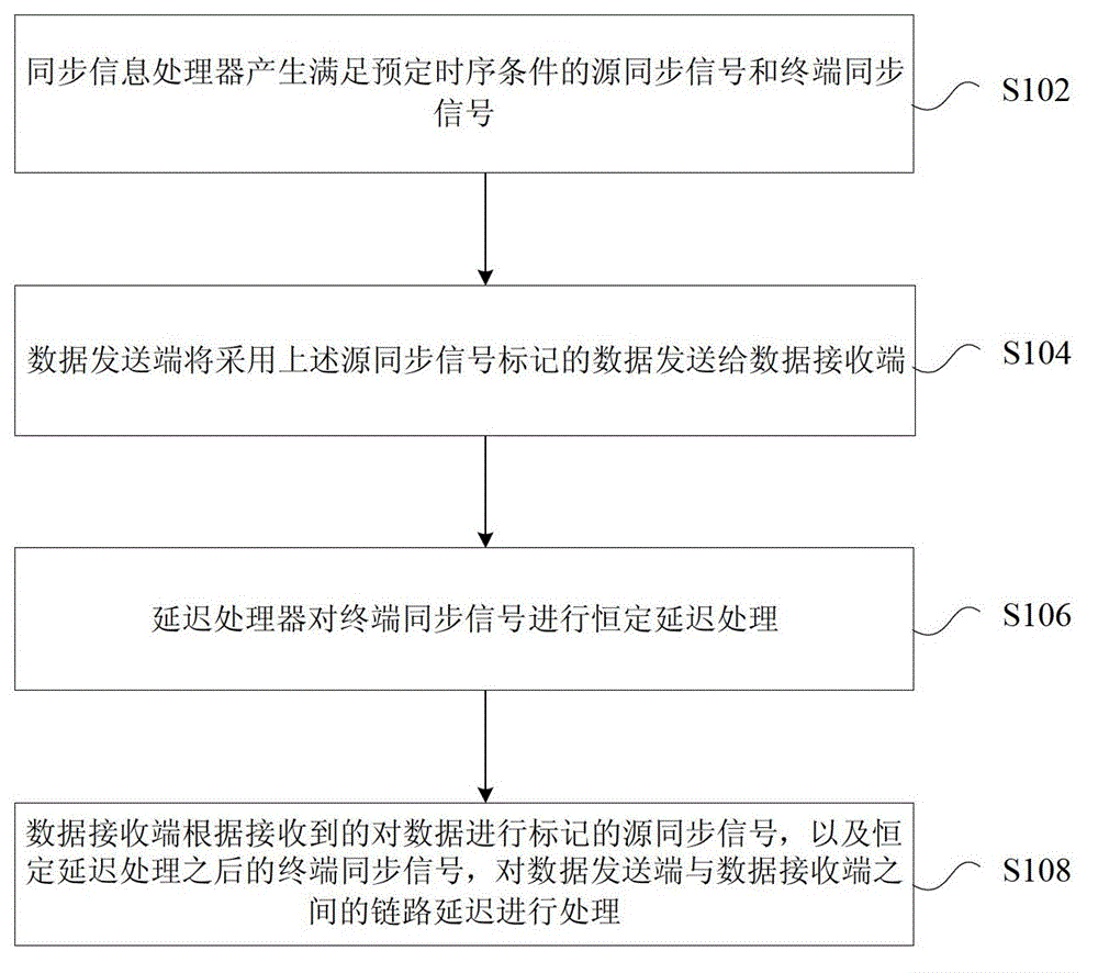
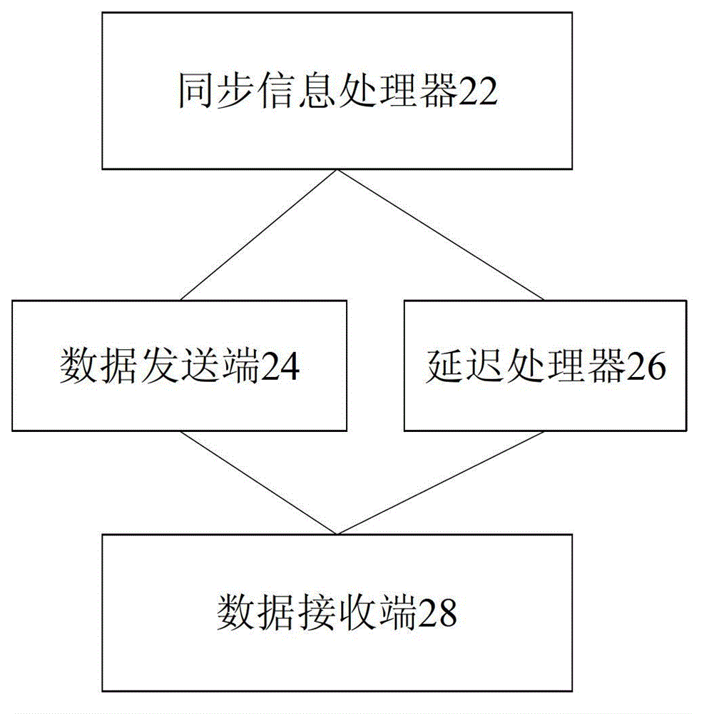
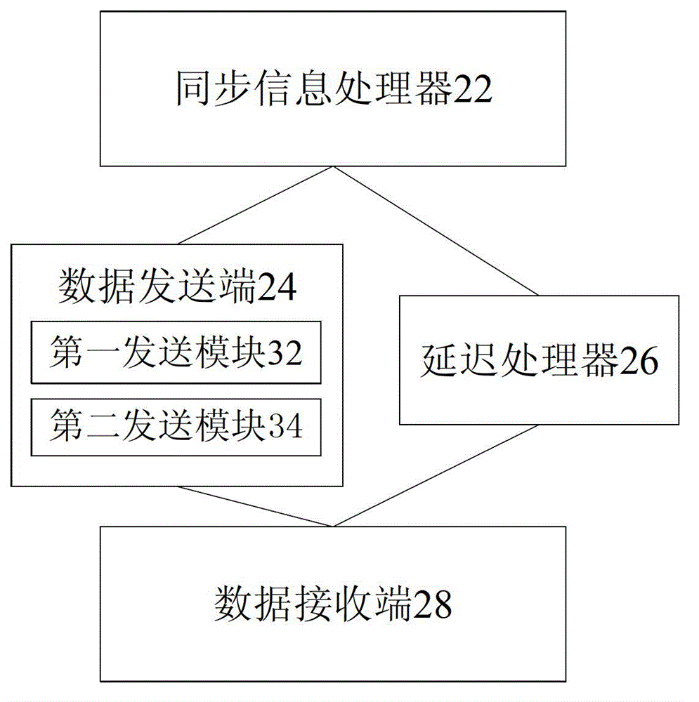
[0028] In this embodiment, a link delay processing method is provided, figure 1 is a flowchart of a link delay processing method according to an embodiment of the present invention, such as figure 1 As shown, the process includes the following steps:

[0029] Step S102, the synchronous information processor generates a source synchronous signal and a terminal synchronous signal satisfying predetermined timing conditions, for example, the source synchronous signal and the terminal synchronous signal may be at least one of the following: a periodic signal, a single pulse signal;

[0030] Step S104, the data sending end sends the data marked with the source synchronization signal to the data receiving...


PUM


Abstract

The invention provides a link delay processing method and device. The method includes the following steps: a synchronization information processor generates a source synchronization signal and a terminal synchronization signal which satisfy predetermined time sequence conditions; a data sending end sends data that adopt source synchronization signal marks to a data receiving end; a delay processor performs constant delay processing on the terminal synchronization signal; the data receiving end processes link delay between the data sending end and the data receiving end according to the received source synchronization signal which marks the data and the terminal synchronization signal after constant delay processing. Through the link delay processing method in the invention, the problem existing in related technology is solved that jitter exists in cross-clock domain delay, and jitter is constantly accumulated in multistage cross-clock domain and exceeds a range, thereby affecting system performance, and achieving an effect of effectively controlling and even completely eliminating link delay jitter of a source end to a terminal.

Description

technical field [0001] The present invention relates to the communication field, in particular, to a link delay processing method and device. Background technique [0002] During the transmission of data streams, physical layer analog domain transmission and link layer multi-level cross-clock domain transmission are often encountered, resulting in uncertain link transmission delays. The difference between the maximum value and the minimum value of the link delay is the jitter of the link delay. Some systems, such as wireless distributed base stations, have strict requirements on jitter. If the jitter exceeds the range, the system may not work properly. [0003] Therefore, in the related art, there is a problem that there is jitter in the cross-clock domain delay, so that the jitter accumulates continuously when multi-stage cross-clock domains cause the jitter to exceed the range and affect the system performance. Contents of the invention [0004] The present invention p...

Claims


Application Information

Patent Timeline
Patent Type & Authority Applications(China)
IPC IPC(8): H04L7/00H04L12/875H04L47/56
Inventor 高贞郝鹏黄灿杨丽宁
Owner SANECHIPS TECH CO LTD
Why Eureka
Try Eureka